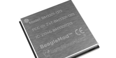
STMicroelectronics has announced mass-production start for its ST67W611M1 combined Wi-Fi 6 and Bluetooth Low Energy 5.4 module, describing the early success of Siana, a lead customer for its fast-to-market connectivity.
The module is the first product of ST’s collaboration with Qualcomm Technologies, announced by the two companies in 2024, to simplify implementing wireless connectivity in systems containing STM32 microcontrollers (MCUs). Their vision, now realised in silicon, fuses ST’s expertise in embedded design and the STM32 ecosystem of microcontrollers, software, and development tools integrated with Qualcomm Technologies’ wireless connectivity technologies.
“Wireless connectivity is a key enabler for the cloud-connected intelligent edge and demand for smart, connected devices continues to expand and accelerate throughout consumer and industrial markets,” said Jerome Vanthournout, Connectivity Business Line Director, STMicroelectronics. “Mastering the complex Wi-Fi and Bluetooth protocols, and bringing that connectivity to devices and IoT applications, are huge challenges. Our modular solution, created with industry-leading knowhow of all aspects, lets product developers focus their resources at the application level and bring new products to market quickly.”
Shishir Gupta, Senior Director, Product Management at Qualcomm Technologies added, “Qualcomm Technologies is thrilled to see the impact of our collaboration with STMicroelectronics through the ST67W module. This module, which contains Qualcomm Technologies’ wireless connectivity components, not only simplifies the integration of Wi-Fi and Bluetooth into a wide range of devices powered by STM32 microcontrollers but also offers incredible flexibility and scalability. This module is a testament to our joint commitment to driving innovation and excellence in the IoT space.”
The ST67W module is ready to integrate with any STM32 MCU and contains a Qualcomm Technologies multiprotocol network coprocessor and 2.4GHz radio. All RF front-end circuitry is built-in, including power/low-noise amplifiers, the RF switch, balun, and integrated PCB antenna, with 4Mbyte Flash for code and data storage and a 40MHz crystal. The module comes pre-loaded with Wi-Fi 6 and Bluetooth 5.4 and is pre-certified according to mandatory specifications. Thread and Matter will be supported soon via software update. There is also an optional coaxial antenna or board-level connections for an external antenna. Security is handled with cryptographic accelerators and services including secure boot and secure debug reaching PSA Certified Level 1, making it easy for customers to comply with the upcoming Cyber Resilience Act and RED directives.
Product developers need no RF design expertise to create a working solution using this module. Highly integrated in a 32-lead LGA package, it is ready to place on the board and permits simple, low-cost PCB designs with as few as two layers.
Siana Systems is among the first IoT technology companies to explore the opportunities this wireless connectivity module brings to enhance product performance and accelerate time to market.
“The ST67W module expands opportunities to add Wi-Fi to devices powered by various STM32 microcontrollers and worry less about the minimum requirements. We can simply integrate the module and quickly get Bluetooth and Wi-Fi connectivity, with minimal additional engineering, which provides us with a simple go-to solution for our next generation designs,” said Sylvain Bernard, Founder and Solution Architect, Siana Systems. “The module’s RF performance, with the radio and front-end circuitry integrated, is very strong, and the flexible power management with fast wake-up times lets us create extremely energy-efficient new products.”
The ST67W611M1 leverages the STM32 ecosystem, which contains over 4,000 commercial part numbers, powerful STM32Cube tools and software, and enhancements that boost edge AI development. The STM32 family covers a broad spectrum from economical Arm® Cortex®-M0+ devices to variants with high-performing cores like Cortex-M55, Cortex-M4 with DSP extensions, and Cortex-A7 in the STM32MP1/2 MPUs.