Renesas introduces eight-pin package for RL78 / G15 MCU 

A general purpose microcontroller (MCU) has been added to the Renesas Electronics low power RL78 family. The small, eight-pin package size targets eight-bit MCU applications, advised Renesas.

The versatile RL78 / G15 packs many peripheral functions and four to 8kbyte of code flash memory in package sizes ranging from eight to 20 pins, with the smallest eight-pin device measuring only 3.0 x 3.0mm. They are designed to keep system size small and reduce the cost of end systems, such as industrial, consumer, sensor control, lighting, and inverter applications. The maximum operating ambient temperature of 125 degree C covers a wide temperature range and allowing the MCU to be used near heat-generating components such as inverter motors.

All pins can be used for general-purpose I/O, except VDD and VSS power supply pins. In addition to up to 8kbyte of code flash memory, the MCU has 1kbyte of code flash memory, 1kbyte of data flash and 1kbyte of SRAM.

It supports operating voltages from 2.4 to 5.5V and supports CSI, UART, Simple I2C, and multi-master I2C serial interfaces. The MCU has a high-precision oscillator (±1.0 per cent) and a built-in comparator.

Engineers designing with the RL78 / G15 can use the GUI-based Smart Configurator to generate driver code for peripheral functions. Renesas also offers the Fast Prototyping Board (FPB) for evaluation, which comes with Arduino Uno and Pmod Type 6A interfaces with access to all pins. Debugging and programming are possible using only a USB cable. Developers can gain access to RL78 development resources using just an Arduino library that can run on the FPB. They can also access the resources offered through the Arduino ecosystem.

The RL78 / G15 is available today in volume production. 

Renesas Electronics combines embedded processing, analogue, power and connectivity expertise to deliver semiconductors for the automotive, industrial, infrastructure and IoT market sectors.

http://www.renesas.com

> Read More

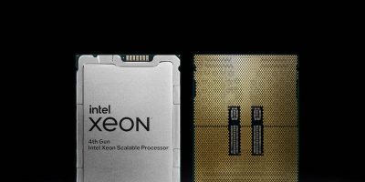
Intel optimises fourth general Xeon Scalable processors for data centre power

The fourth generation Intel Xeon Scalable processors are Intel’s most sustainable data centre processors, said the company. They have a range of features for optimising power and performance, to help achieve customers’ sustainability goals, said Intel.

Code-named Sapphire Rapids, the Xeon processors are claimed to have the most built-in accelerators of any CPU available today, making them suitable for AI, analytics, networking, security, storage and high performance computing (HPC) applications.

Compared to earlier generations, they increase performance per Watt efficiency by a factor of 2.9, using built-in accelerators, to save up to 70W power per CPU in optimised power mode with minimal performance loss, said Intel. This equates to between 52 and 66 per cent low total cost of ownership (TCO).

The number of built-in accelerators means that the fourth generation Xeon processor needs less additional discrete acceleration.

The new optimised power mode can deliver up to 20 per cent socket power savings with a less than five per cent performance impact for selected workloads. Innovations in air and liquid cooling reduce total data centre energy consumption, added Intel. 

The manufacturing process of the processors uses 90 per cent or more renewable electricity at Intel sites with water reclamation facilities.

In AI, and compared to the previous generation, the processors increase PyTorch real time inference and training performance with built-in Intel Advanced Matrix Extension (Intel AMX) accelerators. 

The low latency network and edge workloads mean that the fourth generation Xeon processors are “a critical part of the foundation driving a more software-defined future for industries ranging from telecommunications and retail to manufacturing and smart cities,” said Intel. For 5G core workloads, the built-in accelerators help increase throughput and decrease latency, while the processors’ power management enhances both the responsiveness and the efficiency of the platform, Intel added. 

Compared to earlier generations, they deliver up to twice the virtualised radio access network (vRAN) capacity without increasing power consumption. This enables communications service providers to double the performance-per-Watt to meet critical performance, scaling and energy efficiency needs.

The latest Xeon processor combines up to four Intel 7-built tiles on a single package, connected using Intel EMIB (embedded multi-die interconnect bridge) packaging technology. It delivers increased memory bandwidth with DDR5, increased I/O bandwidth with PCIe5.0 and Compute Express Link (CXL) 1.1 interconnect.

http://www.intel.com

> Read More

NXP targets advanced edge applications with the i.MX 95 family

Part of NXP’s SafeAssure portfolio, the i.MX 95 applications processor family uses an advanced heterogeneous domain design. This not only powers safety-enabled platforms but also integrates a real time safety domain.

The i.MX 95 family combines high performance compute, immersive Arm Mali-powered 3D graphics, a new NXP accelerator for machine learning and high speed data processing. The technology is suitable for automotive, industrial, networking, connectivity and advanced human machine interface (HMI), says NXP. The i.MX 95 family also delivers high performance safety and security features, developed in compliance with automotive ASIL-B and industrial SIL-2 functional safety standards and including an integrated EdgeLock secure enclave.

A critical requirement for the next wave of edge applications is advanced processing and machine learning capabilities, with high-speed connectivity, to analyse the environment and make intelligent decisions locally, explained NXP. The i.MX 95 family is the first i.MX applications processor family to integrate NXP’s eIQ Neutron neural processing unit (NPU). It also includes a new image signal processor (ISP), developed by NXP.

“The i.MX 95 family brings unparalleled features and performance to markets like automotive and industrial where security and safety are key,” stated Rafael Sotomayor, executive vice president and general manager of Secure Connected Edge at NXP. He believed that the combination of processing and graphics, integrated heterogeneous safety domain and networking capabilities, will support “ a new generation of safe and secure edge platforms”.

The i.MX 95 family integrates a secure enclave to simplify implementation of security critical functions in edge applications, such as secure boot, cryptography, trust provisioning, and run-time attestation. Combined with NXP’s EdgeLock 2 GO key management services, manufacturers can securely provision i.MX 95 SoC-based products for secure remote management of devices deployed in the field, including secure over the air updates (OTA), said NXP. 

The i.MX 95’s integrated eIQ Neutron NPU is part of a vision processing pipeline for use with multiple camera sensors or network-attached smart cameras. The SoC integrates an NXP ISP supporting a wide array of imaging sensors to enable vision-capable industrial, robotics, medical and automotive applications, all backed by comprehensive NXP developer support. The Arm Mali GPU enables scaling from multi-display automotive infotainment centres to industrial and IoT HMI-based applications.

The multi-core application domain, with up to six Arm Cortex-A55 cores, is complemented by an independent safety domain consisting of Arm Cortex-M7 and Arm Cortex-M33 CPUs for low power, real time and high performance processing. The i.MX 95 family is designed to enable ISO 26262 ASIL-B and SIL-2 IEC 61508 compliant platforms. Its functional safety domain serves as a critical capability for many automotive and industrial applications. The i.MX 95 can be used in automotiv safety critical actions, for example voice warnings, instrumentation and cameras. In industrial factory automation, the functional safety domain helps to ensure that an industrial control system will always return to a pre-determined state, even when rest of the system fails.

The 10GbE and two 1GbE ports will contribute to industry 4.0, automotive connectivity domain controllers and IoT smart home gateways, said NXP. In addition to time sensitive networking (TSN) capabilities, wireless connectivity (Wi-Fi, Bluetooth Low Energy, satellite radio, or 5G) can be added via two independent PCIe ports, a USB 3 port and integrated BSP-level drivers, said NXP.

Other features include NXP’s Energy Flex architecture that enables fine-grained independent power management of Cortex-A applications domain and real time Cortex-M safety domain. This allows developers to run the real-time safety domain at all times for sensor data monitoring. It also allows the powering up of the applications domain only when necessary to minimise system-level energy consumption.

There is also support for LPDDR5 and LPDDR4X DRAM and multiple options, within the family to scale performance and features to suit power, performance, and application requirements.

The i.MX 95 applications processors are expected to begin sampling for lead customers in 2H 2023.

http://www.nxp.com

> Read More

Renesas releases Wi-Fi development kit supporting new Matter protocol

Renesas has released its first development kit that includes support for the new Matter protocol. Renesas also announced that it will offer Matter support on all future Wi-Fi, Bluetooth Low-Energy and IEEE 802.15.4 (Thread) products, including products from Dialog Semiconductor and Celeno Communications, which it recently acquired.

The Matter securely and robustly connects various smart devices with each other across ecosystems, regardless of the manufacturer to address interoperability conflicts for smart home devices. The application layer protocol abstracts the underlying connectivity technologies such as Wi-Fi, Thread and Bluetooth Low Energy. By using a common software stack, device manufacturers who build with Matter will support various smart home ecosystems and voice services. Smart home users will be able to buy any Matter-certified device regardless of their platform of choice.

Renesas is a member of the Connectivity Standards Alliance. “Connectivity is a critical part of our IoT solutions,” commented Sean McGrath, vice president of the connectivity and audio business division in Renesas’ IoT, industrial and infrastructure business unit. He believed that the company’s broad range of Bluetooth and Wi-Fi solutions, and Thread products in development, mean it is “well positioned to take advantage of the Matter standard in a variety of applications working with customers worldwide.”

Renesas has more than a decade of experience in Bluetooth LE and Wi-Fi. With more than 600 million wireless devices shipped, Renesas offers a broad range of connectivity SoCs used in IoT, wearable products and home networking.

The DA16200 Ultra-Low Power Wi-Fi Modules development kit is based on the DA16200 SoC, believed to be the world’s first Wi-Fi SoC to deliver year-plus battery life for always-connected Wi-Fi IoT devices. 

DA16200 also supports Renesas Quick Connect IoT through the Ultra Low Power Wi-Fi Pmod board. It is fully integrated into Renesas’ e2 studio for easy system development using Renesas MCU, connectivity and other devices. 

Renesas is sampling the DA16200 Development Kit with Matter support to lead customers now and expects to release it broadly by the end Q1 2023.

http://www.renesas.com

> Read More

About Smart Cities

This news story is brought to you by smartcitieselectronics.com, the specialist site dedicated to delivering information about what’s new in the Smart City Electronics industry, with daily news updates, new products and industry news. To stay up-to-date, register to receive our weekly newsletters and keep yourself informed on the latest technology news and new products from around the globe. Simply click this link to register here: Smart Cities Registration