Functional electronic layers can be laid directly on a component, says binder. The binder Innovation & Technology Center has developed the direct printing technique.
As digitisation increases and smart systems proliferate, there is a need for a balance between more complex sensor networks with data processing and simpler, more user friendly operator support, says binder. The trend toward miniaturisation makes it difficult to equip parts due to a limited amount of space with conventional sensors. The binder method of direct printing is claimed to overcome all these challenges. Dr Stefan Ernst, one of the co-developers of the new printing technique, explains: “The printed electronics need less space. In addition, they are more flexible in application and more cost efficient,” he said.
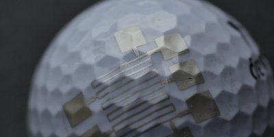
Using a recently developed transfer printing technique, binder was able, for the first time, to apply planar functional electronic layers with a thickness of maximum precision to textured, three-dimensional surfaces in only one printing pass.
Circuit traces, sensors and displays, for example, can be printed without the need for foils or other substrate materials. A protective layer can be overprinted and specially developed nano pastes provide stable parameters for the printing process.
Intended uses in the industrial area range from flexible circuit traces and heating elements to sophisticated sensors. By printing capacitive sensor elements, for example, touch displays of almost any shape can be implemented on three-dimensional and/or textured surfaces. The same approach can also be used for an intuitive gesture control system. Temperature sensors or strain gauges can be implemented by measuring the change in the resistance values of the printed functional layers. The flexible printing technique allows the sensor to be quickly adapted to the application-specific task.
The newly created binder electronic solutions group provides custom-made solutions for connectors, contacts, circuit layout and automatic placement. Services range from design and prototype to series production.