
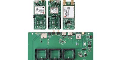
Mouser is now shipping the XPLR-HPG-1 Explorer kit from u-blox. This Explorer kit is comprised of a baseboard populated with a NORA-W106 module, which integrates a powerful dual-core 32-bit microcontroller with 802.11b/g/n Wi-Fi and dual-mode Bluetooth LE 5 connectivity. The baseboard also features three mikroBUS connectors with pre-mounted click boards hosting u-blox positioning and cellular modules. The GNSS RTK 2 click board features the ZED-F9R module, a high-precision dead-reckoning. The LBAND RTK click board includes the NEO-D9S module, a satellite data receiver for the L-band correction broadcast. The 4G LTE 2 click board features the LARA-R6001D, a compact LTE Cat 1 multi-mode module offering global coverage, enabling the reception of PointPerfect correction data via mobile networks. Equipped with its GNSS and communication modules, this Explorer kit can access correction data from a satellite broadcast via L-band satellite GNSS receiver or IP connectivity using LTE or Wi-Fi. PointPerfect, the u-blox GNSS augmentation service, provides correction data delivered via the Thingstream IoT service delivery platform. The XPLR-HPG-1 also supports the Networked Transport of RTCM via Internet Protocol (NTRIP. The XPLR-HPG-1 kit’s modular design also enables users to switch out Mikroe click boards. The Explorer kit provides a flexible, modular development and prototyping platform for centimetre-level accuracy positioning applications, such as autonomous robotics, asset tracking and connected health.
ICs & Semiconductors
Industry-first embedded SIM from ST supports new standard for IoT
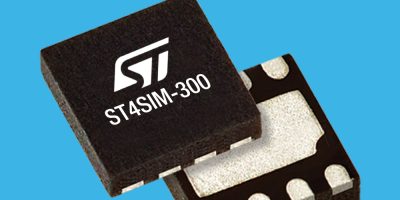
ST has introduced the ST4SIM-300, the first embedded SIM in the industry to meet the incoming GSMA standard for eSIM IoT deployment. Also known as SGP.32, the new standard introduces special features to facilitate managing IoT devices connected to cellular networks.
“Leveraging the incoming GSMA specification, our embedded SIM for IoT solution, ST4SIM-300, enhances flexibility, eases network provider switching, and simplifies managing large numbers of connected devices,” said Agostino Vanore, Edge Authentication and M2M Cellular Marketing Manager at STMicroelectronics. “In a more connected and secured world, it will enable seamlessly track assets across the globe, connect smart devices to the cloud, and securely handle data from billions of devices, supporting our healthcare and smart infrastructures, cities, factories, and homes.”
Unlike existing eSIM machine-to-machine (M2M) and eSIM Consumer specifications, eSIM for IoT (SGP.32) is created for the needs of today’s IoT deployments. ST’s ST4SIM-300 supports features including greater automation of remote SIM provisioning (RSP), easily managing SIM profiles for large fleets of devices, and remote switching between network providers that eliminates physical SIM card swaps. The new eSIM conforms to the latest 5G standard and facilitates deploying devices that have a limited user interface and deploying low-power wide-area network (LPWAN) devices.
ST is sampling ST4SIM-300 eSIMs in various form factors, including wafer-level chip-scale packages (WLCSP) suitable for smart meters, GPS trackers, asset monitors, remote sensors, medical wearables, and similar devices.
Built with an EAL6+ certified ST secure microcontroller, the ST4SIM-300 is architected for security from the ground up. Compatible with GSMA IoT SAFE applet the eSIM facilitates adding secure element features for end-to-end communication and supports scalable security by design for creators of IoT devices.
Alif launches an MCU with AI/ML processing in a tiny footprint
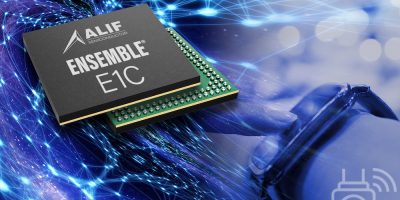
Alif Semiconductor has launched the Ensemble E1C, an MCU series which combines rich digital and analog capabilities with a low-power on-chip neural processing unit (NPU) in a new compact form factor.
This new Ensemble family MCU, which combines a 160MHz Arm Cortex-M55 CPU core with Helium vector processing extension, an Arm Ethos-U55 NPU generating up to 46 GOPs, and up to 2MB of tightly coupled SRAM, is available in a tiny WLCSP package occupying a footprint of 3.9mm x 3.9mm.
The introduction of the E1C extends the Ensemble family, providing a new entry-level option for OEMs that want AI performance and ultra-low power consumption implemented in a familiar Arm environment. The new E1C also shares the same architecture as the Balletto family, allowing for software re-use across the entire family, and easy migration of applications from one device to another.
The E1C can perform both AI/ML and application control functions at ultra-low power levels. This means manufacturers can bring advanced ML capabilities to products such as wearable devices that have extreme constraints on power and space. The E1C’s capabilities are optimised for local ML workloads such as object recognition, speech recognition, sensor fusion, and adaptive audio noise cancellation, easing heavy dependence on the cloud to provide a better user experience.
The high AI performance of the E1C is matched by its power efficiency. The E1C’s aiPM technology can dynamically power only the logic and associated memory that are in use at any given time, thus achieving the lowest overall system power consumption. The aiPM power management unit implements four system-level power modes including a Stop mode which draws just 700nA.
The Ethos-U55 NPU performs 128 MACs/cycle to give ML output of 46 GOPS, and enables on-the-fly weight decompression. This results in inferencing performance some 100x faster and more power-efficient than competing MCUs based on an Arm Cortex-M4 CPU provide. The E1C’s digital cores are backed by up to 2MB of MRAM non-volatile memory alongside up to 2MB of zero wait-state SRAM. A high-speed OctalSPI interface enables expansion to external memory if required. Versions of E1C devices are offered with and without the NPU.
The E1C features a rich set of analog and connectivity peripherals. Two 12-bit SAR ADCs and a 24-bit sigma-delta ADC, a 12-bit DAC and an internal reference voltage provide for fast, precise processing of signals from external sensors. Outputs can be displayed on rich colour displays using a MIPI DSI display interface.
A broad selection of serial communications interfaces includes USB 2.0, SDIO, 2x CAN FD and I3C. Designers of connected devices can also benefit from the same low-power and high-performance characteristics of the E1C with the addition of built-in Bluetooth Low Energy connectivity by choosing the Balletto B1, launched by Alif on 9 April 2024.
Security is a core attribute of the Ensemble family, and the E1C shares the same architecture. Its advanced secure enclave, which provides a solid hardware root-of-trust enabling secure key generation and storage, secure boot, cryptographic accelerators, and certificate management, eliminates the need for an external Secure MCU in endpoint AI devices.
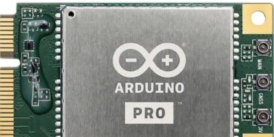
Arduino’s Pro 4G module delivers fast and reliable 4G connectivity worldwide
Mouser Electronics, is now stocking the Pro 4G module from Arduino. Powered by a Quectel LTE Cat 4 modem, the Pro 4G module’s fast data throughput and high bandwidths ensure reliable and quick data download and upload, even in remote locations. The Pro 4G Module expands the connectivity capabilities of Portenta boards for use in smart city infrastructure, industrial automation, fleet management systems, remote maintenance, and other applications.
The Arduino Pro 4G module, now available at Mouser, guarantees reliable 4G connectivity and backward compatibility with existing 2G and 3G networks. The Arduino Pro 4G module connects devices through Arduino Cloud, simplifying error analysis, firmware updates, and remote maintenance. For larger projects such as smart buildings, the modules can be used to remotely monitor temperature, moisture, and deformity levels, accelerating response times when safety is at risk. The Pro 4G module is also an effective connectivity solution in challenging environments, providing long-range coverage and secure data transfer both indoors and outdoors.
Developed in the widely accepted Mini PCIe form factor, the Pro 4G module is compatible with a range of devices for applications, including pipeline monitoring, smart parking, and waste management.
About Smart Cities
This news story is brought to you by smartcitieselectronics.com, the specialist site dedicated to delivering information about what’s new in the Smart City Electronics industry, with daily news updates, new products and industry news. To stay up-to-date, register to receive our weekly newsletters and keep yourself informed on the latest technology news and new products from around the globe. Simply click this link to register here: Smart Cities Registration

