An image recognition SoC for automotive applications has been announced by Toshiba Electronics Europe. It implements a deep learning accelerator at 10 times the speed and four times the power efficiency of Toshiba’s earlier heterogeneous multi-core SoC for image recognition which was introduced at the 2015 IEEE International Solid-State Circuits Conference (ISSCC).
It is designed for advanced driver assistance systems (ADAS), such as autonomous emergency braking, which require increasingly advanced capabilities. Implementing them requires an image recognition SoC that can recognise road traffic signs and road situations at high speed with low power consumption.
Deep neural networks (DNN), algorithms modelled after the neural networks of the brain, perform recognition processing more accurately than conventional pattern recognition and machine learning, and is widely expected to be used in automotive applications. However, DNN-based image recognition with conventional processors takes time, as it relies on a huge number of multiply-accumulate (MAC) calculations. DNN with conventional high-speed processors also consumes too much power, adds Toshiba.
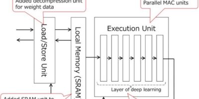
To overcome this, it has developed a DNN accelerator that implements deep learning in hardware. It is defined by three features: parallel MAC units, reduced DRAM access and reduced SRAM access.
The ViscontiTM5 SoC has four processers, each with 256 MAC units to boost DNN processing speed. Conventional SoCs have no local memory to keep temporal data close to the DNN execution unit, they also consume a lot of power accessing local memory and when loading the weight data used for the MAC calculations. In Toshiba’s SoC, SRAM is implemented close to the DNN execution unit, and DNN processing is divided into sub-processing blocks to keep temporal data in the SRAM, reducing DRAM access. Additionally, Toshiba has added a decompression unit to the accelerator. Weight data, compressed and stored in DRAM in advance, are loaded through the decompression unit. This reduces the power consumption involved in loading weight data from DRAM, explains Toshiba.
Finally, conventional deep learning needs to access SRAM after processing each layer of DNN, which consumes too much power. The accelerator has a pipelined layer structure in the DNN execution unit of DNN, allowing a series of DNN calculations to be executed by one SRAM access.
The ViscontiTM5 SoC complies with ISO26262, the global standard for functional safety for automotive applications.
Sample shipments of Toshiba’s image-recognition processor will begin in September 2019.
http://www.toshiba.semicon-storage.com