Ethernet PHY combines security engine with Tbit capacity

Microchip claims to have developed the industry’s first Tbit-scale Ethernet PHY that enables the highest-density 400GbE and FlexE connectivity.

The META-DX1 family of Ethernet physical layer (PHY) devices enables telecomms service providers to build networks using routing and switching to reduce cost, optimise bandwidth and increase capacity. The META-DX1 also integrates the Media Access Control Security (MACsec) security engine.

The device, developed by Microchip’s subsidiary, Microsemi, combines Ethernet ports from 1Gigabit Ethernet (GbE) to 400GbE, Flexible Ethernet (FlexE), Media Access Control Security (MACsec) link encryption and nanosecond timestamping accuracy. Its Tbit capacity is designed to address the industry transition from 100GbE to 400 GbE to support traffic within hyperscale data centres. This traffic volume is expected to quadruple by 2021 (source: Cisco’s Global Cloud Index), with data centre-to-data centre traffic growing at more than a 30 per cent cumulative annual growth rate (CAGR).

The META-DX1 enables line cards to quadruple in capacity, from 3.6Tbits per second to 14.4Tbits per second with 36 ports of 400GbE or 144 ports of 100GbE.

The MACsec engine secures traffic leaving the data centre or enterprise premises. FlexE enables both cloud and telecomms service providers to reduce capex by optimally configuring links beyond today’s fixed-rate Ethernet so they can use low-cost, high-volume optics, while meeting the increasing capacity requirements. Combining the MACsec and FlexE in one device, meets the next phase of capacity scaling in data centre interconnect (DCI) buildouts, adds Microchip.

The META-DX1 is further differentiated in the market with the addition of integrated flexible crosspoint switching, which makes it easier for OEMs to navigate the market transition from 25Gbits per second psnon return to zero (NRZ) and 56Gbits per second pulse amplitude modulation (PAM) -based architectures by enabling them to support a single design or device for both 100GbE (QSFP28) and 400GbE (QSFP-DD) optics. Timestamping is also provided with nanosecond-level accuracy on every port to ensure network builds will meet the challenging timing requirements of 5G mobile basestation deployments.

Initial META-DX1 family members will sample during Q3 2019. All devices are hardware-compatible and supported by the same software developer’s kit.

http://www.microchip.com

> Read More

Microchip claims eSPI to LPC bridge is industry’s first commercial offering

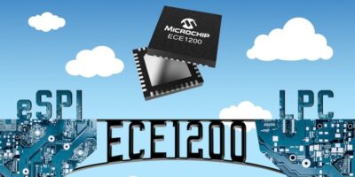
Industrial computing developers can integrate the eSPI standard in existing equipment, using the ECE1200 bridge from Microchip. According to the company, it minimises development costs and extends product lifecycles.

The eSPI bus technology supports new computing with next-generation chipsets and CPUs.

It is believed to be the industry’s first commercially available eSPI-to-low pin count (LPC) bridge. The ECE1200 bridge allows developers to implement the eSPI standard in boards with legacy LPC connectors and peripherals, says Microchip. This allows the developers to implement the eSPI standard while preserving significant investments in legacy LPC equipment and substantially minimising development costs and risk.

The eSPI-to-LPC bridge allows developers to maintain long lifecycles while supporting the eSPI bus technology that is required for new computing applications using the next generation of chipsets and CPUs. To reduce risk for developers, the eSPI bus technology has been through intensive validation for industrial computing applications and has been validated with leading processor companies.

The ECE1200 detects and supports modern standby mode with low standby current. This helps industrial computing developers to manage operating costs and efficiencies. The does not require any software.

To streamline development, the ECE1200 comes with a BIOS porting guide, schematics and a layout guide.

The ECE1200-I/LD is available today in a 40-pin VQFN package.

http://www.microchip.com

> Read More

RX microcontrollers have precision for sensing equipment

The first RX microcontrollers with integral analogue front end have been announced by Renesas Electronics. The RX23E-A microcontrollers are intended for high-precision sensing and measurement equipment.

The 32-bit RX microcontrollers are designed for applications that require high-precision measurements of analogue signals for temperature, pressure, weight, and flow. According to Renesas, they enable such signals to be measured with better than 0.1 per cent precision without calibration.

They achieve analogue front end precision with offset drift of 10 nV/ degrees C, gain drift of one ppm/ degrees C, and RMS noise of 30nV rms. According to Renesas these deliver a level that could previously only be achieved by combining dedicated ADC circuits with high-precision operational amplifier ICs. By integrating high-precision analogue front end intellectual property (IP) on a single chip using the same fabrication process technology, Renesas has made it possible to implement sensor measurement, computation, control, and communication on a single chip to reduce the number of required components, save space, and simplify system design in equipment such as temperature controllers, recording, weighing, and force sensing devices. It also accelerates endpoint intelligence by enabling distributed processing with microcontrollers.

To improve productivity, factories and manufacturing sites are required to measure a variety of sensor data accurately and reliably. For stability when measuring small signals at high precision over a wide environmental temperature range, it is important to reduce noise characteristics and temperature drift characteristics, which prompted Renesas to develop the high-precision analogue front end and integrate it into an RX microcontroller.

The RX23E-A microcontrollers are based on the RXv2 core, which has operating speeds of 32MHz, a digital signal processor (DSP), and superlative floating point unit (FPU) calculations. This allows the implementation of adaptive control using temperature data and inverse matrix calculations using six-axis distortion data.

The company cites the example of robot arm force sensors which require the measurement and calculation of the six-axis distortion in a small space. The RX23E-A microcontrollers make it possible to measure the six-axis distortion data and perform the inverse matrix calculations with a single chip.

The analogue front end block has a 24-bit delta-sigma ADC which has up to 23 bits of effective resolution. Two ADCs can start synchronously, allowing sensor temperature correction to be performed without switching channels.

A rail to rail input programmable gain amplifier allows amplification up to x128, there is also analogue differential inputs of up to six channels (pseudo-differential) and up to 11 channels (single-ended inputs), all of which can be used as inputs to the two ADCs.

The microcontroller block has a 32-bit RXv2 core operating at 32MHz, 128 to 256kbyte of ROM and 16 to 32kbyte of RAM, as well as one SPI, one I2C and one CAN channel and four channels of UART for communication interfaces.

To address functional safety, the software load is reduced by self-diagnostic and disconnection-detection assistance functions for the ADC, clock frequency accuracy measurement circuit, independent watchdog timer and RAM test assistance functions.

Operating temperature is -40 to +85 degrees C and -40 to +105 degrees C.

The RX23E-A microcontrollers are supplied in a 48-pin QFP and 40-pin QFP.

Samples of the RX23E-A microcontrollers are available now with mass production planned for December 2019.

http://www.renesas.com

> Read More

Arm introduces CPU and GPU for 5G mobiles

At Computex in Taiwan this week, Arm has unveiled the latest Cortex CPU, a new Mali GPU. Based on a new architecture and a processor for machine learning.

The latest Cortex CPU, the Cortex-A77 improves instruction per cycle (IPC) performance by 20 per cent, compared with the Cortex-A76 for machine learning, augmented reality and virtual reality (ML, AR and VR).

The Arm Mali-G77 GPU is based on Valhall architecture and is intended for use in mobile devices to deliver graphics at increased efficiency, according to Arm. Microarchitecture enhancements including engine, texture pipes, and load store caches, which achieve 30 per cent better energy efficiency and 30 per cent more performance density. The Valhall architecture is claimed to deliver close to 40 per cent performance improvement compared with the Mali-G76 in devices today.

Arm also says that it boosts inference and neural net (NN) performance for ML and to deliver more immersive games for mobile apps.

A dedicated ML processor delivers up to five tera operations per second (TOPS) per W as part of Project Trillium. The ML processor and open-source Arm NN software framework was announced in 2018 and enhancements to the ML processor include more than double energy efficiency to 5TOPS/W, memory compression improved by up to a factor or three and scaling to peak next-generation performance up to eight cores for up to 32TOPS.

http://www.arm.com

> Read More

About Smart Cities

This news story is brought to you by smartcitieselectronics.com, the specialist site dedicated to delivering information about what’s new in the Smart City Electronics industry, with daily news updates, new products and industry news. To stay up-to-date, register to receive our weekly newsletters and keep yourself informed on the latest technology news and new products from around the globe. Simply click this link to register here: Smart Cities Registration