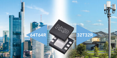
NFC IC provides security tamper detection for IoT applications

Certified security is combined with a tamper status detection mechanism and battery-free sensing in the NTAG 22x DNA StatusDetect IC family by NXP. The ICs measure a change in ambient conditions, such as moisture, liquid fill level or pressure and allow developers to combine secure authentication with opening status detection or condition monitoring of products to help maintain a secure supply chain and product integrity. 

Physical products can be authenticated by leveraging the NTAG 22x DNA IC’s secure unique NFC (SUN) authentication message feature. This allows manufacturers to cost-effectively combat counterfeits and supply chain fraud, said NXP. 

The electronic tamper status detection of the ICs enables manufacturers or product users to verify a product’s unauthorised opening. By measuring capacitive changes in an item’s environmental conditions such as moisture, pressure or fill level, upon a simple tag readout, it is also possible to ensure product quality remains intact or capture digital sensing data for healthcare, retail or industrial applications. 

According to NXP, the inclusion of security-certified NFC sensing turns a tag into a simple battery-less sensing device to detect a physical product’s first opening status, or a change in its specific ambient condition. It can help manufacturers protect product integrity, whilst enabling a new level of intelligence to assure product quality 

The NTAG 22x DNA family is Common Criteria EAL3+ -certified, and features a powerful, cryptographically secure authentication message that dynamically changes on every NFC phone tap, making the taps unclonable, without requiring a user application. 

The NTAG 22x DNA StatusDetect also includes configurable conductive or capacitive tamper detection, with once-open status irreversibly stored and protected in the IC memory without the need for a dedicated app. The conductive mode is suitable for tamper-evident labels and seals fixed on to a product or its package. The capacitive mode is suitable to integrate the tag into a physical product, and is also harder to reconstruct by a fraudster, said NXP.

The StatusDetect ICs can also be used as a passive sensing device to detect an environmental change influencing the capacitance value, interpreted with a mobile or cloud-based application. This facility allows new applications for medical IoT devices, such as a plaster that can detect moisture levels for wound care, fill level sensing for smart injectable dosage devices. It can also be used for consumer products as refill reminders based on package fill levels and leak detection. 

Security features include a 7byte identifier, a SUN message authentication using an AES-128 key and has user memory protected with 32-bit password or with mutual authentication with AES-128 key.

The StatusDetect devices have capacitive measurement with up to 64 granular steps and automated mirroring of UID, NFC counter and status value into IC’s user memory as part of NFC-NDEF message, secured with a SUN message code.

The ICs are available in sawn and bumped wafer format (120 and 75 micron) and with an internal tuning capacitance of 50pF.

http://www.nxp.com

> Read More

Low power photo relays suit smart meter and security systems 

Two normal open 1-Form-A photo relays from Toshiba Electronics combine a MOSFET optically coupled to an infra red LED, making them suitable for a wide range of applications including use in smart meters, passive infrared (PIR) sensors in security systems and building automation applications. The TLP223GA and TLP223J are also intended for use in industrial applications such as programmable logic controllers (PLCs), I/O interfaces and many types of sensors. They can also be used to replace a mechanical relay with a solid-state device.

Both photo relays feature an LED developed by Toshiba with high luminous efficiency, ensuring that the trigger LED current does not exceed 2mA. This reduces energy consumption by approximately 33 per cent, compared to Toshiba’s TLP240x series. Typical on-state resistance is 17Ohm for the TLP223GA and 30Ohm for the TLP223J.

Both the TLP223GA and TLP223J feature an off-state output terminal voltage rating of 400V and 600V respectively. Continuous on-state current (ION) is 120mA and 90mA and pulsed on-state current (IONP) is three times these values.

The two photo relays have improved switching characteristics compared with Toshiba’s previous devices. For example, approximately 50 per cent improvement in turn-on time to 1ms (max) for the TLP223GA, and 75 per cent, 0.5ms (max) for the TLP223J, compared with the TLP240GA and TLP240J.

Operating temperature range is -40 to +110 degrees C, which makes them suitable for use in equipment installed outdoors. The isolation voltage of 5,000V rms and creepage / clearance distances up to 8.0mm allow the photo relays to be used in equipment which requires reinforced isolation, advised Toshiba.

Both devices are housed in a four-pin DIP with leaded and surface mount options available.

The devices are shipping now.

Toshiba Electronics Europe is the European electronic components business of Toshiba Electronic Devices and Storage. It offers European consumers and businesses a variety of hard disk drive (HDD) products as well as semiconductors for automotive, industrial, IoT, motion control, telecomms, networking, consumer and white goods applications. The company’s portfolio encompasses power semiconductors and other discrete devices ranging from diodes to logic ICs, optical semiconductors as well as microcontrollers and application specific standard products (ASSPs).

Toshiba Electronics Europe has headquarters in Düsseldorf, Germany, and branch offices in France, Italy, Spain, Sweden and the United Kingdom providing marketing, sales and logistics services. 

http://www.toshiba.semicon-storage.com

> Read More

JEDEC-compliant multimedia card saves space

Two industrial-grade, embedded multimedia cards (eMMC) have been announced by Alliance Memory. The 4Gbyte ASFC4G31M-51BIN and 8Gbyte ASFC8G31M-51BIN are designed for solid-state storage in consumer, industrial, and networking applications. Each 11.5 mm by 13 mm 153-ball FBGA package integrates NAND flash memory with an eMMC controller and flash transition layer (FTL) management software. 

The devices comply with the JEDEC eMMC v5.1 industry standard, supporting boot operation, replay protected memory block (RPMB), device health report, field firmware updates, power-off notification, enhanced strobe features for faster and more reliable operation, write levelling, high-priority interrupt (HPI), secure trim / erase, and high speed HS200 and HS400 modes. The ASFC4G31M-51BIN and ASFC8G31M-51BIN are also backwards-compatible with eMMC v4.5 and v5.0. 

The eMMCs will be used in products such as smart watches, tablets, digital TVs, set-top boxes, VR and AR headsets, digital cameras, infotainment, CCTV, surveillance, automation, point of sale (PoS) systems, and emerging embedded applications. 

According to Alliance Memory, the eMMCs simplify designs for fast and easy system integration, speeding up product development and time to market. They also save space by eliminating the need for an external controller. The FTL software provides high reliability and stable performance with wear levelling and bad block management. 

The ASFC4G31M-51BIN and ASFC8G31M-51BIN operate over an industrial temperature range of -40 to +85 degrees C and offer programmable bus widths of x1, x4, and x8. The devices’ NAND memory with internal LDO can be powered with a single 3.0V supply voltage, and the controller can be powered by 1.8V or 3.0V dual supply voltages. 

Samples and production quantities of the eMMCs will be available in Q1 2022, with lead times of 12 weeks. 

Alliance Memory provides critical and hard-to-find memory ICs for the communications, computing, consumer electronics, medical, automotive, and industrial markets. The company’s product range includes flash, DRAM, and SRAM memory ICs with commercial, industrial, and automotive operating temperature ranges and densities from 64kbit to 8Gbit. 

http://www.alliancememory.com

> Read More

Zener diodes prolong battery time and save PCB space

Low current regulator diodes are available from Nexperia in three surface mount package options. The 50 microA Zener diodes are available in three surface mountable package options: SOT23 (BZX8450), SOD323 (BZX38450) and SOD523 packages (BZX58550) and leadless DFN1006BD-2 (BZX8850S) package. 

They are also available as Q-portfolio parts, meeting the AEC-Q101 and ISO/TS16949 automotive quality standards. Nexperia explained that more non-automotive applications require additional quality-related services and extended longevity, and these needs will be met by these Q-portfolio parts. 

Specified at a low test current (50 microA), the efficient diodes are ideal for low bias and portable battery-powered devices in mobile, wearable, automotive and industrial applications.

“The DFN1006BD-2 packaged parts with side-wettable flanks (SWF) address the concerns of various sectors, such as size, performance and ruggedness, and match many diverse applications,” says Paula Stümer, product manager at Nexperia. 

There are 40 types per package option covering nominal working voltages from 1.8 to 75V. The Zener diodes feature a non-repetitive peak reverse power dissipation of up to or equal to 40W, total power dissipation up to or equal to 300mW and low dynamic resistance. 

The DFN package dimensions are 1.0 x 0.6 x 0.47mm and are suitable for replacing bulky leaded packages on PCBs. The package can save up to 60 per cent of real estate. It features side-wettable flanks (SWF), which ensure the solder flows up the side of the chip when it is soldered onto the PCB. This technology facilitates automated optical inspection (AOI), satisfying the automotive industry’s high safety, reliability and quality requirements. The high P(tot) of the DFN-packaged Zener diodes also run cooler than leaded parts, therefore improving system reliability.

The 50 microA Zener diodes are available as samples and in volume production quantities. 

Nexperia produces essential semiconductors, with an extensive portfolio which includes diodes, bipolar transistors, ESD protection devices, MOSFETs, GaN FETs and analogue and logic ICs. 

Nexperia, a subsidiary of Wingtech Technology Co., Ltd. (600745.SS), has an extensive IP portfolio and is certified to IATF 16949, ISO 9001, ISO 14001 and ISO 45001. It operates in Asia, Europe and the USA.

http://www.nexperia.com

> Read More

About Smart Cities

This news story is brought to you by smartcitieselectronics.com, the specialist site dedicated to delivering information about what’s new in the Smart City Electronics industry, with daily news updates, new products and industry news. To stay up-to-date, register to receive our weekly newsletters and keep yourself informed on the latest technology news and new products from around the globe. Simply click this link to register here: Smart Cities Registration