Embedded Vision Alliance awards REAL3 image sensor as “Product of the Year”

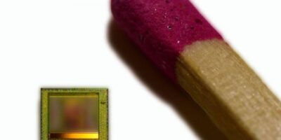
Smartphone cameras increasingly require 3D vision capabilities as differentiating factor. Hence, Infineon Technologies developed the REAL3™ IRS2381C, a premier 3D imager sensor solution especially designed for the mobile device market.

The Embedded Vision Alliance now awarded the 3D Time-of-Flight (ToF) single chip solution as “Product of the Year” in the category “Sensors”. The Award recognises the innovation and achievement of the industry’s leading technologies, services, and products from companies enabling next generation of practical applications for computer vision.

“Congratulations to Infineon for winning Best Sensor in our 2019 Vision Product of the Year awards,” said Jeff Bier, Founder of the Embedded Vision Alliance. “Innovative sensor designs, like Infineon’s 3D Image Sensor, are enabling new 3D vision experiences such as smartphone face recognition and augmented reality. Infineon has been a pioneer in creating 3D image sensors for visual AI applications. I applaud the company’s ongoing investment in innovation and quality in this rapidly changing and often confusing market. I’m proud that Infineon is a member of the Embedded Vision Alliance and delighted they have been recognised with this outstanding honour.”

“We would like to thank the Embedded Vision Alliance for having honoured us with the ‘Product of the Year’ Award, which recognises Infineon’s innovation and performance of our REAL3™ ToF-based 3D imager the category ‘Sensors’, said Philipp von Schierstaedt, Vice President, RF & Sensors, Infineon. “Building upon the combined expertise of Infineon and pmdtechnologies, the novel sensor delivers a new level of 3D camera capabilities in mobile device applications. Infineon’s REAL3TM ToF sensor enables a unique user’s experience in secure face-authentication, computational photography and seamless AR-applications”.

Time-of-Flight (ToF) is the most advanced image sensing technology powering 3D cameras in new generation mobile devices and is posed to fuel the dramatic growth of 3D image sensing application market expected for future years. “Time-of-flight” stands for the time the photons need to travel from the camera to the subject or object of desire and back to the REAL3 sensor. Behind this concept there is unparalleled innovation: it enables the next level of highly secure user smartphone interaction.

The awarded IRS2381C image sensor ensures a high-quality, real time and secure 3D vision experience with supreme performance at all light conditions including outdoor. Compared to other 3D technologies like structured light, Infineon’s 3D ToF technology reduces the number of key components from three to two. Moreover, as distance is measured directly, it requires the least computational resources on the application processor. All this makes the application much more reliable, reduces the size and leads to more competitive costs, while enormously cutting the power drain.

Availability

The new 3D image sensor chip was developed in Graz, Dresden and Siegen and combines the know-how of Infineon’s German and Austrian locations in a single solution. With proven high volume production and a fast, in-factory enabled and lifetime valid calibration process, IRS2381C is the 3D image sensor of choice for 3D camera manufacturing in mobile device applications. More information about Infineon’s 3D image sensor family is available at www.infineon.com/real3.

> Read More

Software development kit streamlines SLAM in mobile devices

To develop simultaneous localisation and mapping (SLAM) –enabled mobile devices, augmented reality/virtual reality (AR/VR) headsets, robots, autonomous vehicles and drones, Ceva offers the SLAM software development kit for CEVA-XM intelligent vision DSPs and NeuPro AI processors

The kit incorporates hardware, software and interfaces that can “significantly lower the entry barrier” to integrate efficient SLAM implementations into low-power embedded systems, says Ceva.

According to Ilan Yona, vice president and general manager of the vision business unit at Ceva: “SLAM is the underlying technology that enables high-accuracy 3D mapping of a device’s surroundings”. He believes that the company’s expertise in designing vision DSPs and software algorithms will introduced customers to 3D machine vision design.

The Ceva-SLAM software development kit has a detailed interface from a CPU to offload the heavy lifting SLAM blocks to the Ceva-XM DSP. These building blocks use the DSP to support both fixed point and floating point math and extend the device’s battery life. They also include capabilities for image processing (including feature detection, feature descriptors, feature matching), linear algebra (including matrix manipulation, linear equation solving) and fast sparse equation solving for bundle adjustment. The software development kit can run a full SLAM tracking module on the Ceva-XM6 DSP at 60 frames per second consuming just 86mW (using a frame size of 1280 x 720, running on Ceva-XM6 using TSMC’s 16nm process).

The software development kit, deployed with a Ceva-XM DSP or a NeuPro AI processor, can be used for visual positioning, classical and neural network workloads for imaging and vision using SLAM.

The Ceva-SLAM software development kit is available for licensing now, exclusively in conjunction with the Ceva-XM intelligent vision DSPs and NeuPro AI processors.

Ceva will presenting the Ceva-SLAM software development kit at the Embedded Vision Summit in Santa Clara, California, USA (Wednesday 22 May).

Ceva licenses signal processing platforms and artificial intelligence processors.  It provides low power IP for vision, audio, communications and connectivity including   DSP-based platforms for LTE/LTE-A/5G baseband processing in handsets, infrastructure and cellular IoT (NB-IoT and Cat-M) enabled devices, imaging and computer vision for any camera-enabled device, audio/voice/speech and low power always-on/sensing applications for IoT markets.

http://www.ceva-dsp.com

> Read More

Rutronik UK supports STM32MP1 processor

System memory for the recently introduced STM32MP1 multi-core microprocessor series includes compute and graphics support combined with power-efficient real-time control. The aim is to aid the development of high-performance solutions for industrial, consumer, smart home, health and wellness applications.

Rutronik UK has combined STM32MP1 technology with approved technology partners Nanya in the form of a 4Gbit DDR3L SDRAM 16-bit and also Toshiba Memory’s 4GByte eMMC. The multi-core microprocessors and the memories, recommended by ST, are available from the distributor.

Engineers can used the STM32MP1 microprocessor series to develop a range of applications using the new heterogeneous architecture that combines up to two Arm Cortex-A7 and a Cortex-M4 core. This flexible architecture performs fast processing and real-time tasks on a single chip, always achieving the greatest power efficiency, reports Rutronik UK. The STM32MP1 embeds a 3D graphics processor unit (GPU) to support human machine interface (HMI) displays.

Rutronik also offers an evaluation board, the STM32MP157C-EV1 and two Discovery kits, the STM32MP157A-DK1 and STM32MP157C-DK2.

A firmware package, STM32CubeMX, is designed for software and hardware configuration of both the Cortex-A7 and Cortex-M4 cores. It handles C-code generation for the M4 core, DDR SDRAM interface configuration, and tuning tool. It can also generate Linux device trees.

Rutronik UK operates as an independent company in the UK. Its parent company, Rutronik Elektronische Bauelemente, is a broadline distributor for semiconductors, passive and electromechanical components in addition to storage technologies, displays and boards and wireless products. The markets that the company primarily targets include automotive, medical, industrial, home appliance, energy and lighting. It also offers support in the areas of product development and design, individual logistics and supply chain management.

http://www.rutronik.com

> Read More

Pressure sensor is sensitive for extended temperatures

A ceramic port is included in the design of the Bourns Model BPS140 pressure sensor to enhance its compatibility with certain harsh media, explains the company.

The pressure sensor is added to Bourns’environmental sensors. It is based on microelectromechanical systems (MEMS) technology, which provides extremely accurate condition readings in a miniature package size. Designed to deliver high sensitivity/accuracy and long-term reliability, the BPS140 pressure sensors offer extended temperature capability and certain harsh media compatibility.

Model BPS140 is robust with a structure that is capable of handling high pressure ranges (15 to 500 PSI) even at high temperatures. This rugged structure is combined with rear pressure measurement that minimises the number of media-sensitive wetted materials. The purpose of this sensing design is to ensure the measured media only touches the back of the measurement element, explains Bourns.

The structure enhances sensor accuracy because all electronic components and other sensitive surfaces are isolated from the media, explains Bourns. In addition, by reducing the number of wetted materials,  the media sensitivity of the sensor is effectively decreased, adds the company.

Bourns’ latest sensor family offers stable performance over the product’s lifespan, and the ability to work with a wide range of pressures offering a total error band of 2.5 per cent full scale over a temperature range of –40 to +150 degrees C (six sigma process), and a lifetime drift of 0.5 per cent full scale. These features make the BPS140 pressure sensor particularly suitable for a range of industrial, energy, heavy equipment, building and home control and medium/low risk medical designs.

Bourns¨ Model BPS140 pressure sensors are available now, and are RoHS** compliant. Bourns also offers port configuration and calibration customisation.

Bourns manufactures and supplies position and speed sensors, circuit protection solutions, magnetic components, microelectronic modules, panel controls and resistive products.

The company is headquartered in Riverside, California, USA, and serves a broad range of markets, including automotive, industrial, consumer, communications, medical (low/medium risk), audio and various other

http://www.bourns.com

> Read More

About Smart Cities

This news story is brought to you by smartcitieselectronics.com, the specialist site dedicated to delivering information about what’s new in the Smart City Electronics industry, with daily news updates, new products and industry news. To stay up-to-date, register to receive our weekly newsletters and keep yourself informed on the latest technology news and new products from around the globe. Simply click this link to register here: Smart Cities Registration