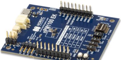
Wireless power receiver from Renesas has WattShare TRx mode

Renesas Electronics has added the P9415-R wireless power receiver to its portfolio. The 15W receiver uses WattShare technology and enables smartphones, power banks, and portable industrial and medical equipment, to wirelessly charge other mobile devices and accessories that also have wireless charging capabilities.

The P9415-R features up to 5W of transmit power capability in transmitter/receiver (TRx) mode, as well as receive up to 15W on Qi transmitters, enabling quick and convenient mobile device charging on the go.

Renesas believes the P9415-R will bring WattShare technology to a wider audience. It combines receiver and transmitter capabilities, allowing smartphones, smart watches, wireless ear buds and other devices to be wirelessly charged simply by placing them on top of a smartphone or other industrial and medical portable devices.

In WattShare TRx mode, the P9415-R enables these mobile devices to change the power flow direction and deliver up to 5W of power to charge other devices. Customers can use the same wireless power coil and same P9415 circuitry to both receive and transmit power wirelessly.

The P9415-R wireless power receiver has an MTP non-volatile memory for easy firmware and device function updates. It also has graphic user interface (GUI) support for user customisation.

It receives up to 30W in proprietary mode and has under voltage lockout down to 2.7V which increases the available charging area and connection times. Sensory accuracy has been improved compared with earlier devices in Renesas’ wireless portfolio to increase foreign object detection capabilities.

The receiver also has bi-directional communications to support proprietary authentication with encryption and x-y alignment circuitry for better receiver/transmitter device alignment.

It is also Renesas’ first WPC 1.3-ready wireless power receiver based on the Wireless Power Consortium’s latest inductive standard.

 Renesas produces both the power receivers (PRx) used in smartphones and other applications, as well as the power transmitters (PTx) used in charging pads and automotive in-car applications.

The P9415-R 15W WattShare wireless power receiver is available now.

http://www.renesas.com

> Read More

Cadence digital and custom tool suite is optimised for TSMC’s 3nm process

The collaboration between Cadence and TSMC has broadened as the partners announce that the former’s digital full flow and custom tool suite has been optimised for TSMC’s 3nm (N3) process technology.

The Cadence tools have achieved the latest design rule manual (DRM) and Spice certification for the N3 process. These innovations assist in driving and delivering next-generation mobile, artificial intelligence (AI) and high performance computing (HPC) applications, developed on the N3 process technology, says Cadence, with reference flows and methodologies.

Customers can download the corresponding N3 process design kit (PDK) to begin design projects now.

The updated digital full flow for N3, features enhanced physical optimisation and timing signoff closure. It includes the Innovus Implementation System, Liberate Characterisation, Liberate Variety Statistical Characterisation, Quantus Extraction Solution, Tempus Timing Signoff Solution, Voltus IC Power Integrity and Pegasus Verification System. In addition, the Genus Synthesis and its predictive iSpatial technology is enabled for these process technologies for mobile, AI and hyperscale designs, adds Cadence.

The digital suite and available reference flows help customers achieve better power, performance and area (PPA) while designing on TSMC’s N3 process. Tool suite enhancements include, improved extraction accuracy, updated routing rules, accurate LVF-generation during characterisation and robust support of advanced colouring.

The certification on TSMC’s N3 process includes the Virtuoso Custom IC design platform, consisting of the Virtuoso Schematic Editor, Virtuoso Layout Suite and Virtuoso ADE Product Suite, the Voltus-Fi Custom Power Integrity Solution, and the Spectre Circuit Simulation Platform, which includes the Spectre X Simulator.

Custom enhancements for TSMC’s N3 process technology include expanded 3nm design rule support, custom digital colour remastering, enhanced analogue cell support, additional productivity improvements with an enhanced device-level place and route flow and a front-to-back legacy-node design migration flow.

Suk Lee, senior director of the Design Infrastructure Management Division at TSMC, commented: “Our latest work enables our customers to design with the tools, benefitting from the significant power and performance boost of TSMC’s 3nm process technology and to quickly launch their new product innovations to market.”

http://www.cadence.com

> Read More

Binder unveils printing technique that gives sensors a new dimension

Functional electronic layers can be laid directly on a component, says binder. The binder Innovation & Technology Center has developed the direct printing technique.

As digitisation increases and smart systems proliferate, there is a need for a balance between more complex sensor networks with data processing and simpler, more user friendly operator support, says binder. The trend toward miniaturisation makes it difficult to equip parts due to a limited amount of space with conventional sensors. The binder method of direct printing is claimed to overcome all these challenges. Dr Stefan Ernst, one of the co-developers of the new printing technique, explains: “The printed electronics need less space. In addition, they are more flexible in application and more cost efficient,” he said.

Using a recently developed transfer printing technique, binder was able, for the first time, to apply planar functional electronic layers with a thickness of maximum precision to textured, three-dimensional surfaces in only one printing pass.

Circuit traces, sensors and displays, for example, can be printed without the need for foils or other substrate materials. A protective layer can be overprinted and specially developed nano pastes provide stable parameters for the printing process.

Intended uses in the industrial area range from flexible circuit traces and heating elements to sophisticated sensors. By printing capacitive sensor elements, for example, touch displays of almost any shape can be implemented on three-dimensional and/or textured surfaces. The same approach can also be used for an intuitive gesture control system. Temperature sensors or strain gauges can be implemented by measuring the change in the resistance values of the printed functional layers. The flexible printing technique allows the sensor to be quickly adapted to the application-specific task.

The newly created binder electronic solutions group provides custom-made solutions for connectors, contacts, circuit layout and automatic placement. Services range from design and prototype to series production.

http://www.binder-connector.de

> Read More

Multi-sensor module is for developers with the IoT bug

SmartBug is an intelligent multi-sensor IoT module by TDK. The InvenSense module combines TDK’s MEMS sensors and precision algorithms in a simple, wireless unit.

It is designed as a dedicated source of smart sensor data for a range of IoT applications from smart homes and appliances to wellness monitoring.

The module enables quick and easy access to reliable and smart sensor data without the need for programming, soldering or extra modifications, says TDK. The SmartBug integrates TDK’s six-axis IMU (gyroscope and accelerometer) with magnetometer, pressure, temperature, humidity and ultrasonic sensors and high-precision algorithms. These algorithms include sensor fusion, HVAC filter monitoring, asset monitoring, gesture detection, activity classification, air mouse monitoring and smart door open/close detection.

The SmartBug module enables accurate and remote monitoring via both Bluetooth Low Energy (BLE) and Wi-Fi and provides autonomous SD card data logging capability for IoT applications with large data volumes.

The SmartBug is small with a flat base and is designed to be placed almost anywhere, from a simple door to an industrial robot for remote data collection. The module can be used by product developers across consumer and commercial IoT applications, advises InvenSense, a TDK Group company.

InvenSense partners Nordic Semiconductor, AKM, Sensirion, and Espressif Systems provide an ecosystem set of components that enable multiple key features within the SmartBug module.

Nordic Semiconductor’s low power microcontroller with BLE 5.2 acquires multi-sensor data from the SmartBug and runs all supported algorithms. It enables streaming of smart sensor data via both USB and BLE, and provides over the air (OTA) firmware upgrades and support for add-on cards with SD card logging and ultrasonic sensors.

The WiFi chip from Espressif Systems expands the wireless data streaming and logging capabilities of SmartBug to higher throughput (up to 2KHz) and long ranges.

AKM’s magnetometer enables multiple features including compass data collection, nine-axis sensor fusion for accurate orientation heading and magnetic anomaly detection for asset monitoring applications in SmartBug.

SmartBug also leverages the humidity and temperature sensor from Sensirion for data streaming and logging, humidity and temperature-based events for asset monitoring applications.

The SmartBug sensor module is currently stocked at TDK’s distribution partners including Arrow, Avnet, DigiKey, Mouser, Symmetry and Components Distributors.

http://invense.tdk.com

> Read More

About Smart Cities

This news story is brought to you by smartcitieselectronics.com, the specialist site dedicated to delivering information about what’s new in the Smart City Electronics industry, with daily news updates, new products and industry news. To stay up-to-date, register to receive our weekly newsletters and keep yourself informed on the latest technology news and new products from around the globe. Simply click this link to register here: Smart Cities Registration