RealWear has announced at the CES that RealWear Navigator Z1, the world’s most advanced intrinsically safe (IS) head-mounted wearable, starts shipping today.
RealWear received its official ATEX / IECEx Intrinsically Safe (IS) certification for RealWear Navigator Z1 (“Navigator Z1”), with consultation with i.safe MOBILE, a technology expert in IS product development. IS certification is granted after passing a plethora of tests (i.e. thermal, electrical integrity, mechanical durability, safety compliance, and explosion-proof testing), validating that the device, whose purpose is to boost productivity and enhance safety for frontline workers, will not cause an explosion where flammable particulates are present in the atmosphere. All consumer electronics that are typically deployed for worker productivity in a standard office environment–including iPhones, tablets, and immersive AR/VR headsets–are strictly prohibited in these zones.
After publicly announcing Navigator Z1 hands-free computing solution, RealWear has received substantial pre-orders from more than a dozen countries in the oil and gas industry, signalling strong product demand globally, including a sizeable order from a major customer in Saudi Arabia.
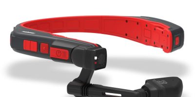
Navigator Z1 are characterised by three distinct benefits:
First, Navigator Z1 represents the pinnacle of RealWear’s product innovation, delivering unparalleled performance with exceptional power efficiency. Navigator Z1 is powered by an advanced Qualcomm SnapDragon 6490 chipset with a built-in advanced AI engine. The platform lays the foundation for RealWear’s broader AI Core vision for frontline workers.
Second, the device now complies with strict ATEX/IECEx certifications. As oil and gas work environments can be extremely noisy, Navigator Z1 ensures voice recognition for fully hands-free use up to 100dBA.
Third, Navigator Z1’s unique modular design, which RealWear pioneered, enables unprecedented customization including the ability to add an IS-certified thermal camera and a swappable battery. The eagerly anticipated Thermal by FLIR thermal camera module is scheduled for release in March.
Customers can purchase the full Navigator series directly via RealWear’s global reseller network. Shipping has commenced in Europe, including UK, Germany, France, Netherlands, and in the United Arab Emirates, as well as across the majority of the Asia-Pacific region including Southeast Asia, Singapore and Australia. Orders in North America, Canada, Japan, Mexico and much of Latin America will be fulfilled in March timeframe for C1D1 zones.
Navigator Z1 is part of the Navigator Series, including Navigator 500 and 520, which are for everyday hands-free work for frontline workers in less restricted work areas.