New, robust approach to overvoltage protection for sensitive electronic signal inputs

High demands on the robustness of electronic systems, especially in industrial environments, continually present developers with great challenges. Overvoltage protection is one key design consideration and challenge, as additional components are usually required to protect systems from overvoltage events – yet they frequently impact and, in the worst case, can even falsify signals. Beyond that, these components incur additional costs and contribute to spatial constraints. Hence, when designing the protection circuit, traditional solutions often require a compromise between system accuracy and the protection level.

Typically, a common and simple design method uses external protection diodes, usually transient voltage suppressor (TVS) diodes, clamped between the signal line and supply or ground. TVS diodes are advantageous as they can react instantaneously to temporary voltage spikes. This type of external overvoltage protection is shown on the left side of Figure 1.

Figure 1. Traditional overvoltage protection design with additional discrete components.
If a positive transient voltage pulse occurs, it is clamped with a current through diode D1 to VDD. The voltage is thereby limited to VDD plus the diode forward voltage. If the pulse is negative and less than VSS, the same applies with the exception that it is clamped to VSS via D2. However, if the leakage current caused by the overvoltage is not limited, it may damage the diodes. For this reason, there is also a current-limiting resistor in the path. For very harsh environmental conditions, an input-side bidirectional TVS diode is often used for enhanced protection.
The disadvantages resulting from this type of protection circuit appear – for example, in the form of increased edge rise and fall times and capacitive effects. Moreover, it doesn’t provide any protection when the circuit is in the de-energised state.
The actual components, such as analogue-to-digital converters (ADCs), operational amplifiers, etc., usually have integrated protection. This can consist of a switch architecture, as shown on the right side of Figure 1. Figure 1 also shows that input-side and output-side protection diodes are present on both supply rails. The downside to this setup is that, when floating signals appear in a de-energized state (the IC is not powered up), the switch may act as if it is active (even if it is set to OFF) as current will flow through the diodes and the power supply rails. This allows current to pass through, resulting in the signal line losing its protection.

Fault-Protected Switch Architecture
One solution to the challenges mentioned above is a fault-protected switch architecture supplemented by a bidirectional ESD cell, as can be seen in Figure 2. Instead of the input-side TVS diodes, now the ESD cell clamps voltage transients by constantly comparing the input voltage with VDD or VSS. In the case of permanent overvoltage, the downstream switch opens automatically. The input voltage is no longer limited by the protection diodes clamped to the supply rails. The limiting factor is now the maximum voltage rating of the switch. Higher system robustness and reliability are additional advantages. There is also virtually no effect on the actual signals and their accuracy. Moreover, the additional current-limiting resistor is not needed because the leakage currents are very low when the switch is open.

Figure 2. Overvoltage protection with integrated bidirectional ESD cell.

This type of input structure is characteristic of the quad SPST (single-pole, single-throw) switch ADG5412F from Analog Devices Inc. (ADI). This switch permits a permanent overvoltage of up to ±55V, regardless of any existing voltage supply. The ESD cell integrated on each of the four channels clamps voltage transients of up to 5.5kV. In an overvoltage condition, only the affected channel is opened and the other channels continue operating normally.

Conclusion
Thanks to this type of overvoltage protection switches, electrical circuits can be greatly simplified. The advantages over the conventional discrete solution are multitudinous, both in terms of guaranteeing optimal switching performance and robustness in a precise signal chain and in terms of spatial optimisation. Hence, the overvoltage protection offered by the ADG5412F is especially suitable for high precision measurement applications in harsh environments.

About the Author
Thomas Brand began his career at Analog Devices in Munich in 2015 as part of his master’s thesis. After graduating, he was part of a trainee program at Analog Devices. In 2017, he became a field applications engineer. Thomas supports large industrial customers in Central Europe and also specialises in the field of Industrial Ethernet. He studied electrical engineering at the University of Cooperative Education in Mosbach before completing his postgraduate studies in international sales with a master’s degree at the University of Applied Sciences in Constance. He can be reached at thomas.brand@analog.com.


> Read More

Isolated pH Monitor with temperature compensation

Introduction

Knowing the pH value of a liquid is essential in many industries. Nearly every industry that handles liquids needs a measurement system for pH. Obviously, it is important for waste water systems and waste water plants, but did you know that the water from a brewery needs to have a special pH value before it reaches the sewage water system? This design tip is intended to help adding high precision isolation to water treatment systems.

This article discusses the addition of high precision isolation to a system. This is essential for monitoring water pH that is located far from the system, monitoring differing ground levels, or for protecting a system from high voltage when an error occurs.

The pH value is a measure of the acidity or basicity of an aqueous solution. It is a unitless number and is defined as the negative common logarithm of the hydrogen ion activity according to the following equation:

Precision isolation is a critical part of water and pH monitoring systems.

Pure water is defined as having a pH value of 7, while acids have values of less than 7 and bases have values above 7. So-called indicators that change colour according to the pH value are often used for measuring the pH. However, this measurement only provides a rough estimate. The circuit shown in Figure 1 is intended for evaluation of combined glass electrodes. It has an accuracy of 0.5% for the pH range from 0 to 14 and is temperature compensated. The circuit supports a large range of pH sensors, which can have high impedance values from 1MΩ to a few GΩ.

Figure 1. pH sensor circuit with combined electrode (simplified).

The pH Electrode

The pH probe consists of a measuring electrode and a reference electrode, which is comparable to a battery. If the probe is dipped into a test solution, the measurement electrode generates a voltage depending on the hydrogen ion activity. A typical output value is 59.14mV per unit of pH at 25°C. Due to the temperature dependency, this value can rise to 70mV/pH. This voltage is compared with the reference electrode. If the test solution is acidic (low pH), the potential at the probe output is greater than 0; for a basic solution, it is less than 0. The output value can be calculated using the following equation:


where:

E is the output voltage of the probe.

E0 is the standard electrode potential (typically 0V), dependent on the probe. R is the universal gas constant. R = 8.31447 J mol−1 K−1.

T is the temperature in Kelvin.

n is the number of transferred electrons (or equivalent number). F is the Faraday constant. F = 96485.34 C mol−1.

pH is the hydrogen ion concentration of unknown solution. pHREF = 7, reference value of reference electrode.

The Circuit

The three main elements of the circuit are the buffer for the probe, the ADC, and the isolator with the voltage transmission. The buffer op amp AD8603 was selected because it has low power consumption, low noise, and extremely low input bias current. The low input bias current of typically 200fA ensures that the voltage drop due to current flow across the internal resistor of the probe is minimised. Another important component is the ADC, represented here by the AD7793, a 24-bit ∑-Δ converter with an integrated power source and programmable amplifier. The integrated current source generates the current that flows through the Pt1000. With this, the temperature measurement needed for compensation in the processor is performed. The same current also flows through the 5kΩ resistor (0.1% tolerance), which thereby generates the reference voltage of 1.05V. As a second function, the resistor boosts the common-mode voltage. Through this and through selection of the reference voltage, the input range of the ADC is fully utilised: the probe outputs ±414mV – a maximum ±490mV. The isolator is the ADuM5411, an isolated dc-to-dc converter that simultaneously provides for isolation of the SPI interface of the ADC.

Circuit Characteristics

To achieve high accuracy, the op amp was selected with a typical input bias current of 200fA, which leads to a maximum voltage offset of 0.2mV at the probe impedance of 1GΩ. This corresponds to an error of 0.0037 units of pH at 25°C. Even with a maximum input bias current of 1pA, the maximum offset error is very low, at 1mV. In order not to give away this good starting position, it is advisable to take suitable layout measurements by using, for example, a guard ring, shielding, and other techniques that are not affected by very low currents. At the selected data rate of 16.7Hz and a gain of 1, the noise generated by the ADC is approximately 2µVrms. If the calculation is done with a peak-to-peak noise of 13µV, the accuracy of the pH value is 0.00022 units of pH. If the noise from the amplifier and the noise from the ADC are taken together, this yields 0.00053 units of pH – and, hence, the offset error is much more significant.

Conclusion

The circuit shown here is a simple, very precise, and power-saving variant for pH sensor readings. Once the circuit has been calibrated, an accuracy of 0.5%, corresponding to 0.005 units of pH can be achieved. Thanks to the isolation, it is suitable for numerous applications.


About the Author

Thomas Tzscheetzsch joined Analog Devices in 2010, working as a senior field applications engineer. From 2010 to 2012, he covered the regional customer base in the middle of Germany and, since 2012, has been working in a key account team with a smaller customer base. After the reorganisation in 2017, he’s leading a team of FAEs in the IHC cluster in CE countries as FAE manager. He can be reached at thomas.tzscheetzsch@analog.com.

> Read More

Accurate, Low Power Remote Sensing Ideas

The remote sensing examples shown here feature high reliability, easy connectivity, and very low power. These circuits target industrial settings that require robust communications and minimal battery maintenance. The solutions combine recent advances in low power, high precision amplification with comparably low power, high reliability wireless mesh network capability. Enabling the solutions are the LTC2063 zero-drift, low input bias amplifier, which runs at 2µA max, and the LTP5901-IPM, which consumes less than 1.5µA in sleep mode. The power dissipation for these devices is low enough that they can run from a benchtop-made battery comprised of copper and zinc electrodes, each four inches square in area, and an electrolyte consisting of the pithy innards of a lemon.

Wireless Mesh

Measurements performed and retrieved on a wireless network in industrial settings rarely require high speeds, but they usually require high reliability and security, in addition to low power operation to maximise battery operating time. The LTP5901-IPM forms a node, or a SmartMesh® IP Mote, in an 802.15.4e wireless network. The LTP5901-IPM integrates a 10-bit, 0V to 1.8V ADC alongside an internal ARM® Cortex®-M3 32-bit microprocessor, which enables sensing with easy programmability. This mote is designed for security, reliability, low power, flexibility, and programmability.

Four Sense Applications

Overall, the design of the following circuits did not require rocket science. Yet, they are tidy, efficient, and well-tailored to specific applications. Complexity is not required and, in fact, would be a cost and reliability hazard.

Each circuit engages a sensor at the input and processes the sensor output to produce an output voltage. With the LTP5901-IPM 10-bit ADC as an input, each circuit tries to map the input to capture much of the 0V to 1.8 Vrange.

Basic Battery Voltage Sense

Figure 1. Simple battery voltage sense.

Figure 1 shows a typical noninverting unity-gain negative feedback op amp configuration that senses a divided-down voltage. The ADC range on the LTP5901 input is 0V to 1.8V. R1 and R2 divide down the battery voltage with minimal quiescent current to enable long lasting battery life. The input bias current of the LTC2063 is low enough that even these large resistance values do not affect the final 10-bit ADC accuracy. The LTC2063 consumes minimal supply current and provides the advantage of zero-drift vs. time and temperature.


Current Sense

Figure 2. Current sense circuit.

The beauty of battery-powered and isolated electronics is the ability to place ground anywhere. One can sense a current in the most convenient circuit topology without loss of generality, while placing the terminals anywhere relative to local ground. For unipolar current such as a 4mA to 20mA industrial loop, one can safely sense relative to local ground using a traditional low-side topology. Figure 2 shows the current flowing through a very small resistor R2, which develops a sense voltage. This input voltage can be extremely small due to the amplifier’s zero-drift, very low valued offset voltage performance. The circuit shown gains up the input developed across a 501mΩ sense resistor by 101V/V. At 20mA, the VOUT is 1.012V. Other values can be chosen to maximise the use of the ADC’s 1.8V range.

Resistance R4 is relatively low and acts as a low impedance shunt of LTC2063 input capacitance. As a consequence, interaction between the large R1 feedback resistor and input capacitance does not play into stability.

The circuit as constructed is optimised for test current ranges from 0mA to 35mA, mapping to the 0V to 1.8V ADC range.

Irradiance Meter

Figure 3. Irradiance measurement using a solar cell in short circuit.

The circuit of Figure 2 can also be used to measure the short-circuit current of a solar cell. Silicon and other solar cells are highly linear in current vs. irradiance when operated in the short-circuit current mode. Short-circuit current is the current from a solar cell with 0V across. The circuit in Figure 3 does not keep the solar cell at precisely 0V at maximum current; however, even with 20mA in full sunlight, the voltage is only 10mV. A 10mV level across the solar cell is virtually a short on its I-V curve.

One might imagine a transimpedance amplifier (TIA) instead. A TIA can force 0V across the solar cell and measure current. The trouble with this kind of circuit is that the op amp supplies the solar cell’s current across the entire range of irradiance. When the priority is minimum power dissipation of the remote sense circuit, 20mA from the battery through the op amp is unacceptable.

Given the need to remain near 0V, a small sense resistor should be used. A remotely located, battery-powered sense of small voltages once again suggests the use of a very accurate, low power amplifier such as the LTC2063.

Solar installations result in exactly the sorts of physical layouts that demand wireless mesh networking with zero temperature drift measurement. Fortunately, silicon photodiodes, in the short-circuit condition, are fairly stable vs. temperature. A simple and robust design utilising the LTC2063 and LTP5901-IPM, combined with a silicon solar cell, is the ideal solution to sensing across a large installation field with changing ambient temperature conditions.

Temperature Measurement with Thermocouple

Figure 4. Thermocouple sense circuit.

Thermocouple voltages can be positive or negative. The circuit of Figure 4 combines the use of a micropower reference and a micropower amplifier to sense tiny voltages that are both positive and negative. It is fortunate that a thermocouple, if electrically isolated from its device under test (DUT), can be placed at whatever voltage domain is convenient. The example in Figure 4 biases the thermocouple at 1.25V by using the LT6656-1.25. The circuit output is a very highly gained version of the small thermocouple voltage on top of a 1.25V reference. The ADC range of 0V to 1.8V is a reasonable target for this configuration. The extremely high gain of roughly 2000V/V would not be feasible without the employment of a zero-drift, low offset amplifier.

Conclusion

Extremely low power, accurate, remote sensing is absolutely attainable. The examples shown in this article reveal the simplicity of combining a low power, high accuracy amplifier with a programmable system-on-chip wireless mesh node.


About the Author

Aaron Schultz is an applications engineering manager in the LPS business unit. His multiple system engineering roles in both design and applications have exposed him to topics ranging across battery management, photovoltaics, dimmable LED drive circuits, low voltage and high current dc-to-dc conversion, high speed fiber optic communication, advanced DDR3 memory R&D, custom tool development, validation, and basic analog circuits, while over half of his career has been spent in power conversion. He graduated from Carnegie Mellon University in 1993 and MIT in 1995. By night he plays jazz piano. He can be reached at aaron.schultz@analog.com.

> Read More

Monolithic full bridge autoresonant transmitter IC simplifies wireless battery charger design

The use of batteries in everyday devices is getting more ubiquitous. In many of these products, a charging connector is difficult or impossible to use. For example, some products require sealed enclosures to protect sensitive electronics from harsh environments and enable convenient cleaning or sterilisation. Other products may simply be too small to include a connector, and in products where the battery-powered application includes movement or rotation, forget about charging with wires. Wireless charging adds value, reliability, and robustness in these and other applications.

There are many ways to deliver power wirelessly. Across a short distance of less than a few inches, capacitive or inductive coupling is commonly used. In this article, solutions using inductive coupling are discussed.

In a typical inductively coupled wireless power system, an ac magnetic field is generated by a transmit coil, which then induces an alternating current in a receive coil just like a typical transformer system. The main difference between a transformer system and a wireless power system is that an air gap or other nonmagnetic material gap separates the transmitter and receiver. Furthermore, the coupling coefficient between the transmit coil and the receive coil is typically very low. Whereas a coupling of 0.95 to 1 is common in a transformer system, the coupling coefficient in a wireless power system varies from 0.8 to as low as 0.05.


Wireless Battery Charging Basics

A wireless power system is composed of two parts separated by an air gap: transmit (Tx) circuitry, including a transmit coil, and receive (Rx) circuitry, including a receive coil.

When designing a wireless power battery charging system, a key parameter is the amount of power that actually adds energy to the battery. This received power depends on many factors including:

  • Amount of power being transmitted
  • Distance and alignment between the transmit coil and the receive coil, commonly represented as the coupling factor between the coils
  • Tolerance of the transmit and receive components

The main goal in any wireless power transmitter design is the ability for the transmit circuit to generate a strong field to guarantee delivery of the required received power under worst-case power transfer conditions. However, it is equally important to avoid thermal and electrical overstress in the receiver during best-case conditions. This is especially important when output power requirements are low and the coupling is great. An example would be a battery charger when the battery is fully charged with a receive coil placed close to the transmit coil.


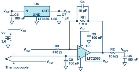
A Simple but Complete Transmitter Solution Using the LTC4125

The LTC4125 transmitter IC is designed to pair with one of the various battery charger ICs in the Power by Linear™ portfolio as the receiver; for example, the LTC4120 – a wireless power receiver and battery charger IC.

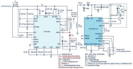
Figure 1. LTC4125 driving a 24μHz transmit coil at 103kHz, with 1.3A input current threshold, 119kHz frequency limit, and 41.5°C transmit coil surface temperature limit in a wireless power system with LTC4120-4.2 as a 400mA single cell Li-Ion battery charger at the receiver.

The LTC4125 comes with all of the features necessary for a simple, powerful, and safe wireless power transmitter circuit. In particular, it has the ability to adjust its output power, depending on the receiver load requirement, as well as to detect the presence of a conductive foreign object.

As mentioned earlier, the transmitter in a wireless battery charger system needs to generate a strong magnetic field in order to guarantee delivery of power under worst-case power transfer conditions. To meet this goal, the LTC4125 employs a proprietary autoresonant technology.

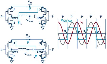
Figure 2. LTC4125 autoresonant drive.

The LTC4125 autoresonant drive ensures that the voltage at each SW pin is always in phase with the current into the pin. Referring to Figure 2, when current is flowing from SW1 to SW2, switches A and C are on while switches D and B are off, and vice versa in reverse. Locking the driving frequency cycle by cycle with this method ensures that the LTC4125 always drives the external LC network at its resonant frequency. This is true even with continuously changing variables that affect the resonant frequency of the LC tank such as temperature and the reflected impedance of a nearby receiver.

With this technology, the LTC4125 continually adjusts the driving frequency of the integrated full bridge switches to match the actual resonant frequency of the series LC network. In this fashion, the LTC4125 is able to efficiently build a large amplitude ac current in the transmitter coil without the need of a high dc input voltage, nor of a highly precise LC value.

The LTC4125 also adjusts the pulse width of the waveform across the series LC network by varying the duty cycle of the full bridge switches. By adjusting the duty cycle higher, more current is generated in the series LC network and therefore more power is available to the receiver load.

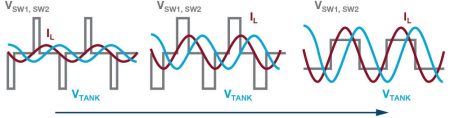
Figure 3. LTC4125 pulse width sweep – voltage and current in the Tx coil increases as the duty cycle is increased.

The LTC4125 performs a periodic sweep of this duty cycle to find the optimum operating point for the load condition at the receiver. This optimum power point search allows operation tolerant of a large air gap and misalignment of the coils while avoiding thermal and electrical over- stress to the receiver circuit in all cases. The period between each sweep is easily programmable with a single external capacitor.

The system shown in Figure 1 is quite tolerant of considerable misalignment. When the coils are misaligned significantly, the LTC4125 is able to adjust the generated magnetic field strength to ensure that the LTC4120 receives the full charge current. In the system shown in Figure 1, up to 2W can be transmitted at a distance of up to 12mm.

Foreign Conductive Object Detection

Another essential feature of any viable wireless power transmit circuit is the ability to detect the presence of a conductive foreign object placed in the magnetic field generated by the transmit coil. A transmit circuit designed to deliver more than a few hundred milliwatts to the receiver needs the ability to detect the presence of conductive foreign objects in order to prevent eddy current from forming in the object and causing undesirable heating.

The autoresonant architecture of the LTC4125 allows a unique method for the IC to detect the presence of a conductive foreign object. A conductive foreign object reduces the effective inductance value in the series LC network. This causes the autoresonant driver to increase the integrated full bridge driving frequency.

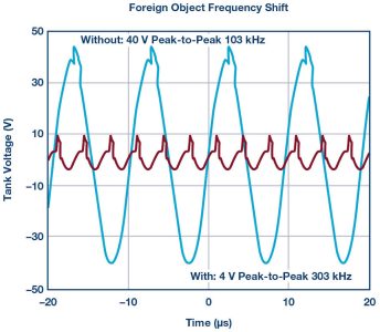
Figure 4. Comparison of the LTC4125 transmitter LC tank voltage frequency with and without the presence of a conductive foreign object.

 By programming a frequency limit via a resistor divider, the LTC4125 reduces the driving pulse width to zero for a period of time when the autoresonant drive exceeds this frequency limit. In this fashion, the LTC4125 stops delivery of any power when it detects the presence of a conductive foreign object.

Note that by using this frequency shift phenomenon to detect the presence of a conductive foreign object, the detection sensitivity can be directly traded off with the component tolerance of the resonant capacitor (C) and the transmit coil inductance (L). For a typical 5% initial tolerance on each of the L and C values, this frequency limit can be programmed at 10% higher than the expected natural frequency from the typical LC value for a reasonably sensitive foreign object detection and robust transmitter circuit design. However, tighter tolerance 1% components can be used with the frequency limit set at only 3% higher than the typical expected natural frequency for a higher detection sensitivity while still maintaining the robustness of the design.

Power Level Flexibility and Performance

With some simple resistor and capacitor value changes, the same application circuit can be paired with a different receiver IC for higher wattage charging.

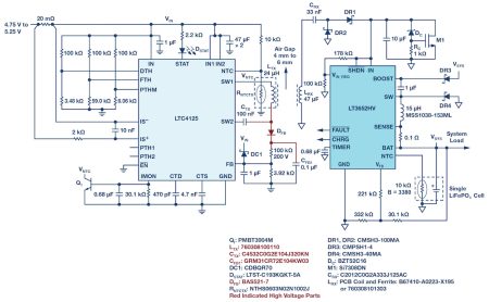
Figure 5. A diagram of the LTC4125 driving a 24μHz transmit coil at 103kHz, 119kHz frequency limit, and 41.5°C transmit coil surface temperature limit in a wireless power system with LT3652HV as a 1A single cell LiFePO4 (3.6V float) battery charger at the receiver.

Due to the high efficiency full bridge driver on the transmit circuit, as well as the high efficiency buck switching topology of the receive circuit, overall system efficiency as high as 70% can be achieved. This overall system efficiency is calculated from the dc input of the transmit circuit to the battery output of the receive circuit. Note that the quality factor of the two coils, as well as their coupling, is just as important to the overall efficiency of the system as the rest of the circuit implementation.

All of these features in the LTC4125 are achieved without any direct communication between the transmitter and receiver coils. This allows for a simple application design, covering various power requirements up to 5W as well as many different physical coil arrangements.

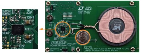
Figure 6. Typical complete wireless power transmitter board using LTC4125.

Figure 6 showcases the small overall size of the typical LTC4125 application circuit as well as its simplicity. As mentioned before, most of the features are customisable using external resistors or capacitors.

Conclusion

The LTC4125 is a powerful IC that provides all of the features necessary to make a safe, simple, and highly efficient wireless power transmitter. The autoresonant technology, optimum power search, and the conductive foreign object detection via frequency shift ease the design of a full-featured wireless power transmitter with excellent distance and alignment tolerance. The LTC4125 is a simple and exceptional choice in a robust wireless power transmitter design.

About the Author

Eko Lisuwandi has been a design engineer at the Analog Devices Boston Design Center since 2002. Eko spent his early career developing supervisory and high voltage power path mixed-signal products in CMOS technology. Later on, his interest expanded to include multichannel bipolar power converters. Now as a technical asset manager and section lead, Eko’s responsibility includes research, design, and development of battery chargers and wireless power integrated circuits in BiCMOS. He received his B.S. in 2001 and M.Eng. degree in 2002, both in electrical engineering and computer science from MIT. He can be reached at eko.lisuwandi@analog.com.

> Read More

About Smart Cities

This news story is brought to you by smartcitieselectronics.com, the specialist site dedicated to delivering information about what’s new in the Smart City Electronics industry, with daily news updates, new products and industry news. To stay up-to-date, register to receive our weekly newsletters and keep yourself informed on the latest technology news and new products from around the globe. Simply click this link to register here: Smart Cities Registration