NFC chip is first IC certified for CCC applications

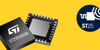
Believed to be the first NFC Forum-certified IC for CCC applications, the ST25R3920B eases certification of digital car key systems, said STMicroelectronics.

The automotive-qualified NFC reader ICs for Car Connectivity Consortium (CCC) digital-key applications is used in car door and centre console locations for keyless entry and starting. It can also be used as Qi wireless-charging control and smartphone pairing. 

The chip has ST’s Heartbeat algorithm for NFC card protection on Wireless Power Consortium (WPC) applications, which can differentiate between an NFC card and a smartphone in card-emulation mode. This ensures phones can charge while cards stay protected.

New features include enhanced active wave shaping (AWS), this eases certification to the latest NFC Forum Certification Release 13 (CR13), said ST. It also promotes interoperability between CCC digital keys and smartphones. AWS helps remove undershoot and overshoot from the received signal by adjusting parameters. In doing so it avoids repeatedly rematching the antenna during development. The ST25R3920B also supports automatic antenna tuning and automatic low power wake up.

The ST25R3920B has output power up to 1.6W combined with what is claimed to be best in class sensitivity to maximise interaction distance when installed in, for example, in a car door handle, where space constraints require a small antenna. The output power is dynamically adjustable to comply with upper and lower limits expressed in NFC Forum and EMVCo specifications.

ST has combined a highly noise-resistant input structure and integrate noise suppression receivers (NSR). It claimed that the ST25R3920B has the market’s best immunity against external interference. It can also pass car manufacturers’ most stringent proprietary injected noise tests to ensure safe operation in worst-case conditions, said the company.

Samples of the ST25R3920B are available now. 

http://www.st.com

> Read More

Space-qualified quad core processor enhances imaging

Qualified flight models of Teledyne e2v’s LS1046-Space processor, based on Arm’s Cortex-A72. It targets compute-intensive space applications, including high throughput satellites and data compression, as well as artificial intelligence and imaging. According to the company, it outperforms existing alternatives by a factor of 30. 

The LS1046-Space processor has minimal power consumption with a data processing performance that makes it suitable for deployment in power constrained Cubesat and Microsatellite platforms where an advanced data path design and access to multiple integrated peripherals are required. 

“With its advanced processing capabilities, powerful feature set, and ease of use and implementation in space systems – it is an important enabler for artificial intelligence and machine learning. It especially suits future, low earth orbit (LEO) operations,” commented Thomas Guillemain, marketing and business development manager for digital products at Teledyne e2V.

Clocked at up to 1.8GHz, the 64bit LS1046-Space processor delivers 30k DMIPs and has a fast, 2.1Gtransfers per second, 64bit DDR4 SDRAM controller with embedded eight-bit error corrected code (ECC). There is also a 2Mbyte L2 cache shared across the four Arm cores. L1 and L2 caches also benefit from ECC-protection, providing a high degree of in-flight immunity to data corruption, said the company. 

A range of embedded interfaces include 10Gbit Ethernet, three PCI-Express (PCIe) v.3.0 lanes, SPI, I2C and multiple UARTs. The device is supplied in a compact 23 x 23mm, 780-ball BGA package.

The LS1046-Space has a wide operating temperature range (-55 to 125 degrees C) and achieves 100krad total ionising dose tolerance. Immunity to single event latch-up (SEL) and upsets (SEU) is being validated in qualification. The processor is qualified up to NASA level 1.

Teledyne e2v’s supplies standard, semi-custom or full custom devices to customers in healthcare, life sciences, space, transportation, defence and security and industrial markets. 

The company will be exhibiting at electronica in Munich (15 to 18 November) with a stand in Hall C4-215; and at Space Tech Expo Europe in Bremen (15 to 17 November) stand number M52 in Bremen, Germany. 

http://www.teledyne.com

> Read More

NXP releases RFCMOS radar transceivers for ADAS and AD

Second generation radar transceivers from NXP are now available for ADAS (advanced driver assistance systems) and AD (autonomous driving). The TEF82xx series of 77GHz RFCMOS radar transceivers is optimised for fast chirp modulation, and supports short-, medium- and long-range radar applications, including cascaded high-resolution imaging radar. 

It enables 360 degree sensing for critical safety applications, including automated emergency braking, adaptive cruise control, blind-spot monitoring, cross-traffic alert and automated parking.

Radar is used for sensing in passenger vehicles’ ADAS but also in MaaS (mobility as a service) applications, says NXP. Fully autonomous driving will demand higher RF performance for distances beyond 300m, as well as at finer resolutions down to sub-degree level to accurately detect, separate and classify smaller objects. Used with NXP’s scalable family of S32R radar processors, NXP said the TEF82xx RFCMOS radar transceivers are able to deliver the fine angular resolution, processing power, and ranges, required for production-ready imaging radar solutions.

The RFCMOS transceivers have three transmitters, four receivers, ADC conversion, phase rotator and low phase noise VCOs (voltage controlled oscillators). It also includes built-in safety monitors and external interface capability for MIPI-CSI2 and LVDS and complies with ISO26262 and ASIL Level B standards.

NXP has doubled RF performance compared with the first generation devices, with improvements such as a +6dB phase noise improvement, output power of 14dBm at phase noise of -95dBc/Hz and a receiver noise figure of 11.5dB. TEF82xx transceivers use a compact eWLB package with exposed die, which optimises heat transfer to meet demanding thermal conditions, even at elevated ambient temperatures. A particularly short chirp return time of just four microseconds reduces power on time to reduce sensor power consumption. It also allows chirps to be spaced more closely in time which increases speed estimation capabilities.

Developers can easily build and optimise applications using the radar algorithm library offered by the automotive-grade radar software development kit (RSDK) without having to spend time manually fine-tuning accelerator software. There is also a large ecosystem of compilers, development environments, MCALs, and both free and commercial RTOS support.

http://www.nxp.com

> Read More

ClockMatrix delivers Class D compliance for O-RAN S-plane Requirements

The 8A34001 system synchroniser is part of Renesas’ ClockMatrix family of precision timing. It is used in AMD’s Zynq UltraScale+ RFSoC DFE ZCU670 evaluation kit and reference design for 5G New Radio (5G NR) and generates low jitter, precision timing signals based on the IEEE 1588 precision time protocol (PTP) and synchronous Ethernet (SyncE).

It exceeds next-generation 5G radio requirements including synchronisation and offers full ITU-T G.8273.2 T-BC/T-TSC class C and D compliance. Renesas offers open source SYNCE4L and PCM4L, that is built on open source PTP4L, and device drivers already in a Linux kernel for the 8A34001. Alternative solutions rely on proprietary software that can be difficult for end customers to integrate and customise on to their software platforms.

The AMD ZCU670 is an evaluation and development platform based on Zynq UltraScale+ RFSoC DFE, the latest AMD silicon for 5G NR targeting both FR1 and FR2 (mmWave) O-RAN applications. 

The 8A34001 performance has been verified on the ZCU670 evaluation platform and has been shown to exceed the 5G system requirements, reported Renesas. The relevant compliance reports and test results are available from Renesas on request. The 8A34001 system synchroniser will be made available as part of the AMD O-RAN reference design where it is used to implement the S-plane functionality in an O-RU reference design. 

Renesas offers a broad silicon timing portfolio in the industry, including a wide range of buffers, oscillators and clock synthesiser products, to resolve timing challenges in wireless infrastructure, networking, data centres and consumer applications. 

The AMD Zynq UltraScale+ RFSoC DFE ZCU670 evaluation kit is available today for qualified customers. The entire ClockMatrix family of timing devices is available from Renesas and its authorised distributors. 

http://www.renesas.com 

> Read More

About Smart Cities

This news story is brought to you by smartcitieselectronics.com, the specialist site dedicated to delivering information about what’s new in the Smart City Electronics industry, with daily news updates, new products and industry news. To stay up-to-date, register to receive our weekly newsletters and keep yourself informed on the latest technology news and new products from around the globe. Simply click this link to register here: Smart Cities Registration