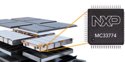
Four LPDDR4X SDRAMs halve power consumption

Four SDRAMs by Alliance Memory combine low voltage operation with fast clock speeds. The fourth generation LPDDR4 SDRAMs range from 2Gbit to 16Gbit.

The latest additions to the company’s high speed CMOS mobile low power LPDDR4X SDRAMs are the 2Gbit AS4C128M16MD4V-062BAN, the 4Gbit AS4C256M16MD4V-062BAN, the 8Gbit AS4C512M16MD4V-053BIN and the 16Gbit AS4C512M32MD4V-053BIN. According to Alliance Memory, they deliver approximately 50 per cent lower power ratings in the 200-ball FBGA package for higher power efficiency. 

They have low voltage operation of 0.6V, lower than 1.1V for LPDDR4 SDRAMs, to increase battery life in portable electronics for the consumer, commercial, and industrial markets, including smartphones, smart speakers, security surveillance systems, and other IoT devices utilising AI and 5G technologies. They also provide increased efficiency for advanced audio and high resolution video in embedded applications. The LPDDR4X SDRAMs deliver clock speeds up to 1.86GHz for high transfer rates of 3.7Gbits per second. 

For automotive applications – including ADAS – the AEC-Q100-qualified AS4C128M16MD4V-062BAN and AS4C256M16MD4V-062BAN offer a temperature range of -40 to +105 degrees C and on-chip ECC for increased reliability. The AS4C512M16MD4V-053BIN and AS4C512M32MD4V-053BIN operate over an industrial temperature range of -40 to +85 degrees C. 

The AS4C512M16MD4V-053BIN, AS4C128M16MD4V-062BAN and AS4C256M16MD4V-062BAN are organised as single channel devices each consisting of eight banks of 16 bits; the AS4C512M32MD4V-053BIN offers two channels. All four components provide fully synchronous operation; programmable read and write burst lengths of 16, 32, and on the fly; and selectable output drive strength. An on-chip temperature sensor controls the self-refresh rate. 

Alliance Memory’s LPDDR4X SDRAMs are designed as drop-in, pin-for-pin-compatible replacements for use in high bandwidth, high performance memory system applications, eliminating the need for costly redesigns and part requalification. 

Samples and production quantities of the new LPDDR4X SDRAMs are available now, with lead times of 12 weeks. 

Alliance Memory provides critical and hard-to-find memory ICs for the communications, computing, consumer electronics, medical, automotive, and industrial markets. The company’s product range includes flash, DRAM, and SRAM memory ICs with commercial, industrial, and automotive operating temperature ranges and densities from 64Kbit to 16Gbyte. 

Privately held, Alliance Memory maintains headquarters in Kirkland, Washington, USA and regional offices in Europe, Asia, Canada, and South America. 

http://www.alliancememory.com

> Read More

High density source measure unit accelerates semiconductor characterisation

The PZ2100 series is high density precision source measure unit (SMU) that accelerates time to market with flexible software options, said Keysight. It provides 20 precision SMU channels within a 1U rack space to speed the characterisation of IC designs.

Designing a semiconductor component or device and delivering it to market remains a time-intensive, technical process, observed Keysight. Digital development engineers must connect and test multiple ports on a single device under test (DUT) throughout the design cycle to troubleshoot and characterise the performance of the IC. High density, automated characterisation prevents engineers slowing their delivery timelines as they validate with complex, multi-port designs using complicated and low density test setups, the company continued.

The PZ2100 series SMU is scalable to 20 SMU channels in a 1U rack configuration. Cooling spacers are not required when stacked. There are five SMU module options available that are configurable and upgradeable.

Keysight said time is saved by simplifying channel stacking and synchronisation to remove integration and coding complexity. The graphic user interface (GUI) accelerates test prototyping, debugging, and troubleshooting. The PathWave IV Curve Measurement software enables quick measurements and synchronisation without programming.

The all-in-one SMU module also reduces cost by integrating pulser and digitiser functions with conventional SMU functions, such as precise DC voltage and current sourcing and measuring. According to Keysight, it meets emerging requirements without additional instruments.

Keysight specialises in design, emulation, and test solutions to help engineers develop and deploy faster, with less risk, throughout the entire product lifecycle. It serves customers in communications, industrial automation, aerospace and defence, automotive, semiconductor, and general electronics markets.

http://www.keysight.com

> Read More

Overcoming Constraints: Design a Precision Bipolar Power Supply on a Simple Buck Controller

Industrial, automotive, IT, and networking companies are major purchasers and consumers of power electronics, semiconductors, devices, and systems. These companies use the full array of available topologies for dc-to-dc converters that employ buck, boost, and SEPIC in different variations. In an ideal world, these companies or firms would use a specialised controller for each new project. However, adopting new chips requires significant investment due to the lengthy and costly process of testing new devices for compliance with automotive standards, verification functionality in the specific applications, conditions, and equipment. The obvious solution for reducing development and design cost is employing already approved and verified controllers in different applications.

The most used topology for generating a power supply is for step-down converters. However, employment of this topology is limited to generating positive outputs from the input voltages that are greater than the output. It cannot be used in a straightforward way for generating negative voltages or providing stable outputs when the input voltage drops below the output. Both aspects to generating output are important in automotive electronics when negative voltage is needed for supplying amplifiers or when a complete system must continuously work properly in case of cold cranking when the input voltage rails drop significantly. This article details a method for using a simple buck controller in SEPIC, Cuk, and boost converters.

Generating Negative and Positive Voltage from a Common Input Rail

Figure 1 illustrates the design of a bipolar power supply based on a single buck controller with two outputs.

Figure 1. An electrical schematic of LTC3892 that is generating positive and negative voltages. VOUT1 is 3.3V at 10A and VOUT2 is –12V at 3A.

For maximum utilisation of this chip, one output must be employed to generate a positive voltage and a second to generate negative voltage. The input voltage range of this circuit is 6V to 40V. The VOUT1 generates positive 3.3V at 10A and VOUT2 negative voltage –12V at 3A. Both outputs are controlled by U1. The first output VOUT1 is the straightforward buck converter. The second output has a more complex structure. Because VOUT2 is negative relative to GND, the differential amplifier U2 is employed to sense negative voltage and scale it to the 0.8V reference. In this approach, both U1 and U2 are referenced to the system GND, which significantly simplifies the power supply’s control and functionality. The following expressions help to calculate the resistor values for RF2 and RF3 in case a different output voltage is required.

The VOUT2 power train employs a Cuk topology, which is widely covered in the relevant technical literature. The following basic equations are required to understand the voltage stress on the power train components.

The VOUT2 efficiency curve is presented in Figure 2. The LTspice® simulation model of this approach is available here. In this example, the LTC3892 converter’s input is 10V to 20V. The output voltages are +5V at 10A and –5V at 5A.

Figure 2. Efficiency curve of the negative output at 14V input voltage.

Generating Stable Voltages from a Fluctuating Input Rail

The electrical schematic of the converter shown in Figure 3 supports two outputs: VOUT1 with 3.3V at 10A and VOUT2 with 12V at 3A. The input voltage range is 6V to 40V. VOUT1 is created in a similar fashion, as shown in Figure 1. The second output is a SEPIC converter. This SEPIC converter, as with Cuk above, is based on non-coupled, dual discrete inductor solutions. Use of the discrete chocks significantly expands the range of the available magnetics, which is very important for cost-sensitive devices.

Figure 3. Electrical schematic of LTC3892 in a SEPIC and in buck applications.

Figure 4 and Figure 5 illustrate the functionality of this converter at voltage drops and spikes; for example, at cold cranking or load dumps. The rail voltage VIN drops or rises at a relatively nominal 12V. However, both VOUT1 and VOUT2 stay in regulation and provide a stable power supply to the critical loads. The two-inductor SEPIC converter can be easily rewired to a single inductor boost converter.

Figure 4. If the rail voltage drops from 14V to 7V, both VOUT1 and VOUT2 stay in regulation.

Figure 5. The rail voltage rises from 14V to 24V. However, both VOUT1 and VOUT2 stay in regulation.

The relevant LTspice simulation model can be found here. It shows the LTC3892 converter’s input is 10V to 20V. The output voltages are +5V at 10A and –5V at 5A.

Conclusion

This article explained the methods of building bipolar and dual-output power supplies based on the step-down controller. This approach allows for the use of the same controller in buck, boost, SEPIC, and Cuk topologies. This is very important for vendors of automotive and industrial electronics, as they can design power supplies with a variety of output voltages based on the same controller, once it is approved.

Author

Victor Khasiev [victor.khasiev@analog.com] is a senior applications engineer at ADI. Victor has extensive experience in power electronics both in ac-to-dc and dc-to-dc conversion. He holds two patents and has written multiple articles. These articles relate to the use of ADI semiconductors in automotive and industrial applications. They cover step-up, step-down, SEPIC, positive-to-negative, negative-to-negative, flyback, forward converters, and bidirectional backup supplies. His patents are about efficient power factor correction solutions and advanced gate drivers. Victor enjoys supporting ADI customers, answering questions about ADI products, designing and verifying power supply schematics, laying out print circuit boards, troubleshooting, and participating in testing final systems.

> Read More

Nordic Semiconductor PMIC for embedded BLE is available from Rutronik

The nPM1300 power management IC (PMIC) from Nordic Semiconductor is now available at Rutronik. The IC integrates essential functions required for embedded Bluetooth Low Energy designs with hard reset functions for one or two buttons, accurate battery indication, a system level watchdog, power failure warning, and recovery from a failed startup in a single device. The level of integration and compact package reduces the number of components required and simplifies system design, said Rutronik.

It is designed to provide efficient power control for Nordic’s nRF52 and nRF53 series SoCs and ensures support for wireless networks such as Bluetooth LE, Thread, Zigbee or Low Energy Audio. 

The nPM1300 is also power efficient and includes accurate measurement functions for monitoring charge level and estimating battery life. It can be used with USB-C compatible chargers for lithium-ion, lithium polymer, and lithium iron phosphate batteries up to 1000mAh. The nPM1300 has four individually controllable power rails including two high performance buck regulators with a 200mA current limit and two 100mA load switches or 50mA LDOs. The PMIC has an operating temperature range of -40 degrees C to +85 degrees C.

The battery charger complies with JEITA and has a termination range of 3.5 to 4.45V and charge current from 32 to 800mA. The input regulator has an input range of 4.0 to 5.5V and output from 4.0 to 5.5V unregulated. USB current limit is 1500mA and the design includes overvoltage protection at 22V transient. 

Other features include an input regulator with USB support, an 800mA charger, ship- and hibernate modes and five general purpose I/Os and three LED drivers.

The nPM1300 PMIC can be used in a choice of applications for wearable devices, handheld entertainment devices, personal health and medical devices and rechargeable smart home sensors.

Rutronik Elektronische Bauelemente was founded in 1973 and is an independent family-owned company based in Ispringen, Germany. It has over 80 offices worldwide and logistics centres in Austin (Texas), Shanghai, Singapore, and Hong Kong, for comprehensive customer support in Europe, Asia and North America. 

The company focuses on high-growth future markets, identified as advanced materials, advanced measurement, processing and analytics, advanced robotics, automation, biotechnology, energy and power, future mobility, IIoT and internet of everything, industry 4.0, medical and healthcare, and transportation, logistics and supply chain.

To serve customers in these future markets, the Rutronik Automotive, Embedded, Power, Smart and System Solutions groups bundle expertise, specific product portfolios, and consultancy support. The services range from competent technical support in product development and design-ins, through the diverse product portfolio of leading manufacturers, to the company’s software and hardware solutions with partly patented Rutronik IP.

http://www.rutronik.com

> Read More

About Smart Cities

This news story is brought to you by smartcitieselectronics.com, the specialist site dedicated to delivering information about what’s new in the Smart City Electronics industry, with daily news updates, new products and industry news. To stay up-to-date, register to receive our weekly newsletters and keep yourself informed on the latest technology news and new products from around the globe. Simply click this link to register here: Smart Cities Registration