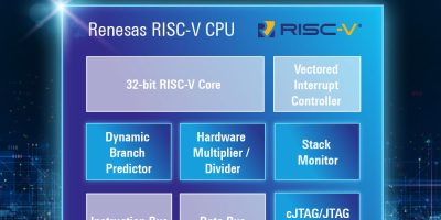
Renesas has announced that it has designed and tested a 32-bit CPU core based on the open-standard RISC-V instruction set architecture (ISA). Renesas is among the first in the industry to independently develop a CPU core for the 32-bit general-purpose RISC-V market, providing an open and flexible platform for IoT, consumer electronics, healthcare and industrial systems. The new RISC-V CPU core will complement Renesas’ existing IP portfolio of 32-bit microcontrollers (MCUs), including the proprietary RX Family and the RA Family based on the Arm Cortex-M architecture.
RISC-V is an open ISA which is quickly gaining popularity in the semiconductor industry, due to its flexibility, scalability, power efficiency and open ecosystem. While many MCU providers have recently created joint investment alliances to accelerate their development of RISC-V products, Renesas has already developed a new RISC-V core on its own. This versatile CPU can serve as a main application controller, a complementary secondary core in SoCs, on-chip subsystems, or even in deeply embedded ASSPs. This positions Renesas as a leader in the emerging RISC-V market, following previous introductions of its 32-bit voice-control and motor-control ASSP devices, as well as the RZ/Five 64-bit general purpose microprocessors (MPUs), which were built on CPU cores developed by Andes Technology Corp.
“Renesas takes pride in offering embedded processing solutions for the broadest range of customers and applications,” said Daryl Khoo, Vice President of the IoT Platform Division at Renesas. “This new core extends our leadership in the RISC-V market and uniquely positions us to deliver more solutions that accommodate a diverse range of requirements.”
“We congratulate Renesas on achieving its recent milestone in 32-bit RISC-V MCU architecture development,” said Calista Redmond, CEO at RISC-V International. “This achievement exemplifies how RISC-V ecosystem partners, such as Renesas, are rapidly advancing RISC-V innovation. Our RISC-V community now spans 70 countries with more than 4,000 members, and we eagerly anticipate further innovations emerging from this dynamic, expanding market.”
The Renesas RISC-V CPU achieves an impressive 3.27 CoreMark/MHz performance, outperforming similar architectures on the market. It includes extensions to improve performance, while reducing code size.
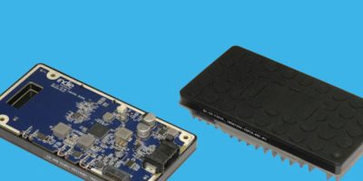
Renesas is sampling devices based on the new core to select customers, with plans to launch its first RISC-V-based MCU and associated development tools in Q1 2024. Details of the new MCU will be published at that time. More information about RISC-V solutions is available at: renesas.com/risc-v.