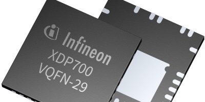
Renesas announces ultra-fast MRAM test chip for IoT and AI devices

Renesas has announced that it has developed circuit technologies for an embedded spin-transfer torque magnetoresistive random-access memory (STT-MRAM, hereinafter MRAM) test chip with fast read and write operations. Fabricated using a 22-nm process, the microcontroller unit (MCU) test chip includes a 10.8-megabit (Mbit) embedded MRAM memory cell array. It achieves a random read access frequency of over 200 MHz and a write throughput of 10.4-megabytes-per-second (MB/s).

As IoT and AI technologies continue to advance, MCUs used in endpoint devices are expected to deliver higher performance than ever. The CPU clock frequencies of high performance MCUs are in the hundreds of MHz, so to achieve greater performance, read speeds of embedded non-volatile memory need to be increased to minimise the gap between them and CPU clock frequencies. MRAM has a smaller read margin than the flash memory used in conventional MCUs, making high speed read operation more difficult. On the other hand, for write performance, MRAM is faster than flash memory because it requires no erase operation before performing write operations. However, shortening write times is desirable not only for everyday use, but also for cost reduction of writing test patterns in test processes and writing control codes by end product manufacturers.

MRAM reading is generally performed by a differential amplifier (sense amplifier) to determine which of the memory cell current or the reference current is larger. However, because the difference in memory cell currents between the 0 and 1 states (the read window) is smaller for MRAM than for flash memory, the reference current must be precisely positioned in the centre of the read window for faster reading. The newly developed technology introduces two mechanisms. The first mechanism aligns the reference current in the centre of the window according to the actual current distribution of the memory cells for each chip measured during the test process. The other mechanism reduces the offset of the sense amplifier. With these adjustments, faster read speed is achieved.

Furthermore, in conventional configurations, there is large parasitic capacitance in the circuits used to control the voltage of the bitline so it does not rise too high during read operations. This slows the reading process, so a Cascode connection scheme is introduced in this circuit to reduce parasitic capacitance and speed up reading.

Thanks to these advances, Renesas can achieve the world’s fastest random read access time of 4.2 ns. Even taking into consideration the setup time of the interface circuit that receives the MRAM output data, we can realize the random read operation at frequencies in excess of 200 MHz.

For the write operation, the high-speed write technologies for embedded STT-MRAM announced in December 2021 improved write throughput by first applying write voltage simultaneously to all bits in a write unit using a relatively low write voltage generated from the external voltage (IO power) of the MCU chip through a step-down circuit, and then used a higher write voltage only for the remaining few bits that could not be written. This time, Renesas takes into account that because the power supply conditions used in test processes and by end product manufacturers are stable, the lower voltage limit of the external voltage can be relaxed. Thus, by setting the higher step-down voltage from the external voltage to be applied to all bits in the first phase, write throughput can be improved 1.8-fold.

Combining the above new technologies, a prototype MCU test chip with a 10.8Mbit MRAM memory cell array was fabricated using a 22 nm embedded MRAM process. Evaluation of the prototype chip confirmed that it achieved a random read access frequency of over 200 MHz and a write throughput of 10.4 MB/s at a maximum junction temperature of 125°C.

The test chip also contains 0.3 Mbit of OTP (Note 2) that uses MRAM memory cell breakdown to prevent falsification of data. This memory can be used to store security information. Writing to OTP requires a higher voltage than writing to MRAM, making it more difficult to perform writing in the field, where power supply voltages are often less stable. However, by suppressing parasitic resistance within the memory cell array, this new technology also makes writing in the field possible.

https://www.renesas.com

> Read More

Infineon introduces lower cost Bluetooth long-range module for low power applications

Infineon has announced the CYW20822-P4TAI040, its latest Bluetooth module that pushes the low-power and range boundaries for wireless connectivity in IoT and consumer electronics. This module offers seamless integration, enhanced performance with Bluetooth low-energy long-range (LE-LR) support, and exceptional reliability for a wide range of applications. With the right combination of low power and high performance, Infineon’s CYW20822-P4TAI040 is designed to support the entire spectrum of Bluetooth LE-LR use cases including industrial IoT applications, smart home, asset tracking, beacons and sensors, and medical devices.

According to a recent report by ABI Research future use cases will demand additional improvements across almost all metrics. These include industrial IoT applications such as sensing, robotics, beacons, smart home, and asset tracking. In response, Infineon’s CYW20822-P4TAI040 Bluetooth module delivers unparalleled connectivity and performance, enabling customers to create innovative products in the IoT and consumer electronics space.

With extensive experience in delivering certified Bluetooth and Bluetooth LE modules, Infineon’s regulatory testing (FCC, ISED, MIC, CE) and certification process with the Bluetooth SIG is precise and rigorous. Its pre-certified modules are optimised for cost, size, power, and range.

“Infineon is thrilled to expand its Bluetooth portfolio with the introduction of the CYW20822-P4TAI040 Bluetooth module to help designers get to market faster,” said Anurag Chauhan, Director of Marketing for the Bluetooth product line at Infineon Technologies. “As a leader in the IoT area in delivering innovative new Bluetooth LE solutions, this new module is a testament to our customer commitment. This new module delivers low power, long range, and excellent RF performance to meet our customers evolving needs.”

Infineon’s CYW20822-P4TAI040 Bluetooth LE module is currently sampling. More information is available at https://www.infineon.com/CYW20822-P4TAI040

> Read More

u-blox introduces new LTE-M modules with integrated GNSS to boost industrial connectivity  

u-blox has announced two new LTE-M cellular module series, the SARA-R52 and LEXI-R52. These modules, designed for industrial applications, are based on the u-blox UBX-R52 cellular chip and are tailored for integrated and concurrent positioning and wireless communication needs. Typical IoT use cases include fixed and mobile applications such as metering and utility, asset tracking and monitoring, as well as healthcare.

A set of new features embedded within the u-blox UBX-R52 chip will allow users to dispense with additional components to design their products. SpotNow is a new positioning feature unique to u-blox, which provides position data with a 10 m accuracy within a couple of seconds. It is meant for occasional tracking applications such as recycling waste dumpsters, elderly trackers, or cleaning machines. The uCPU feature allows users to run their own software within the chip without using an external MCU. The uSCM (Smart Connection Manager), on the other hand, is designed for automatic connectivity management to achieve either best performance or lowest power consumption, for example when a connection is lost and needs to be re-established.

The new u-blox R52 series also introduces a new combo module designed to offer simultaneous GNSS and cellular connectivity – an important attribute for applications requiring continuous or cyclic tracking. The u-blox SARA-R520M10 combo module comes equipped with an integrated u-blox M10 GNSS receiver and ensures concurrent tracking with low-power consumption, better TTFF, and improved RF sensitivity. It is tailored for users who seek the simplicity of a pre-integrated cellular and GNSS solution.

Many LTE-M modules only offer an RF output power of 20-21 dBm, whereas the new R52 series offers 23 dBm, ensuring stable connectivity in challenging coverage conditions. The LEXI-R52 provides the same features as the SARA-R52, but in a smaller form factor (16 x 16 x 2 mm), ideal for ultra-small applications like wearables.

Samples are available now, with volume production scheduled for Q3 2024.

https://www.u-blox.com

> Read More

Infineon presents hybrid Time of Flight technology for next-generation smart robots

In collaboration with device manufacturer OMS and pmdtechnologies, an expert in Time of Flight (ToF) technology, Infineon has developed a new high-resolution camera solution that enables enhanced depth sensing and 3D scene understanding for next-generation smart consumer robots. The new hybrid Time of Flight (hToF) solution combines two depth sensing concepts and helps significantly reduce maintenance effort and costs for smart robots.

Infineon’s REAL3 flexible ToF imager technology enables the combination of established high-resolution iToF flood illumination and dToF long-range spot illumination in a single hybrid Time of Flight camera. For many years now, this high-resolution technology has been used to see the smallest objects in the path of the robot and navigate around them. Adding precise long-range spot data now also allows creation of an accurate 3D map of the surrounding area for intelligent path planning experiences even in challenging light conditions of bright sunlight or darkness that empower the next-generation robot vacuum cleaner.

The new solution reduces the height of robot vacuum cleaners by 20-30 percent, fully replacing the top-mounted LDS (Laser Distance Scanner) making it possible to clean even under furniture with low clearance. Measuring only 31x16x8 mm, the hybrid ToF camera requires much less space for improved mapping and obstacle avoidance functionality. Making multiple sensors redundant, hybrid ToF reduces system costs as well as operation costs, since there are no moving parts that wear out over time.

The solution serves customers with a simplified and user-friendly approach to implementation. The compact hybrid ToF solution is versatile and robust and aligns well with the evolving needs of mobile consumer robot devices in various industries such as robot vacuum cleaners, commercial robots, air-purifiers and size measurement.

https://www.infineon.com

> Read More

About Smart Cities

This news story is brought to you by smartcitieselectronics.com, the specialist site dedicated to delivering information about what’s new in the Smart City Electronics industry, with daily news updates, new products and industry news. To stay up-to-date, register to receive our weekly newsletters and keep yourself informed on the latest technology news and new products from around the globe. Simply click this link to register here: Smart Cities Registration