ST has introduced the first product of its strategic collaboration with Qualcomm Technologies to simplify development of next-generation wireless solutions for industrial and consumer IoT applications. The collaboration aims to deliver initially IoT modules leveraging ST’s powerful STM32 ecosystem and Qualcomm Technologies’ leading wireless connectivity solutions.
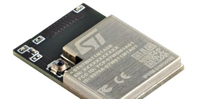
The first of these modules, the ST67W611M1, contains a Qualcomm® QCC743 multiprotocol connectivity system-on-a-chip (SoC), pre-loaded with Wi-Fi6, Bluetooth 5.3 qualified, and Thread combo, made easy to integrate with any STM32 microcontroller (MCU) or microprocessor (MPU). The module will support Matter protocol over Wi-Fi for future-proof connectivity, making the STM32 portfolio seamlessly accessible to the Matter ecosystem. Aiding the system integration, the module also contains 4Mbyte Flash for code and data storage, and a 40MHz crystal. There is also an integrated PCB antenna or micro RF (uFL) connector for an external antenna.
“Our collaboration delivers multiple advantages for the large community that leverage the STM32 family in their embedded systems,” said Remi El-Ouazzane, President, Microcontrollers, Digital ICs and RF Products Group (MDRF) at STMicroelectronics. “Qualcomm’s expertise in highly influential and widely used wireless connectivity technologies is now at product developers’ fingertips and combines with the powerful software, tools, features and project acceleration offered by the STM32 development ecosystem.”
“This is just the beginning of our mission, which we expect to deliver many further successes enabling new and advanced edge processing applications,” said Rahul Patel, Group General Manager, Connectivity, Broadband and Networking Business Unit, Qualcomm Technologies, Inc. “We look forward to continuing our collaboration with STMicroelectronics to bring more unparalleled connected experiences with Wi-Fi, Bluetooth, AI, 5G and more.”
Advanced hardware security is built in, with hardware cryptographic accelerators, as well as services including secure boot and secure debug, reaching PSA Certified Level 1 protection. The module is self-contained and pre-certified according to mandatory specifications, requiring no RF design expertise from the user to create a working solution. Highly integrated in a 32-lead LGA package, it is ready to place on the board and permits simple, low-cost PCB designs with as few as two layers.
The ST67W611M1 leverages the STM32 ecosystem, which contains over 4,000 commercial part numbers, powerful STM32Cube tools and software, and enhancements that boost edge AI development. AI enhancements include the recently introduced STM32N6 MCUs, which contain ST’s Neural-ART Accelerator, and the ST Edge AI Suite that provides an AI Model Zoo and STM32Cube.AI and NanoEdge AI optimisation tools.
The modules are designed to be quickly and seamlessly integrated with any STM32 microcontroller or STM32 microprocessor, which offer flexible options for performance, price, and power across a broad spectrum. The MCUs available range from cost- and power-sensitive devices containing the Arm® Cortex®-M0+ core to devices containing high performing cores such as Cortex-M4 and Cortex-A7 in the STM32MP1/2 MPUs.
Samples of the ST67W611M1 are available, with OEM availability in Q1 2025, with broader availability in Q2 2025.