Rohm has begun offering samples of the industry’s smallest terahertz (THz) wave oscillation and detection devices utilising semiconductor elements known as Resonant Tunneling Diodes (RTDs). Terahertz waves are anticipated to be applied to non-destructive testing, imaging, and sensing in the medical and healthcare sectors, as well as potentially future ultra-fast communication technologies. Providing these devices contributes to the advancement of terahertz wave applications.
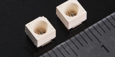
Rohm has developed a 0.5mm × 0.5mm RTD chip for terahertz wave generation and detection, capable of oscillating and detecting terahertz waves at a frequency of 320GHz (typ.) with an output power ranging from 10 to 20µW. Rohm will begin offering samples of this RTD element mounted in a PLCC package (4.0mm × 4.3mm) commonly used for LEDs. With an extremely compact size, typically one-thousandth of that of conventional oscillators, this innovation enables easy development of terahertz wave applications, even in space-constrained environments.
By positioning the antenna surfaces of the oscillation and detection devices facing each other 10mm apart, a dynamic range of 40dB (typ.) can be achieved. Both oscillator and detector maintain a drive power consumption of 10mW (typ.), while their ability to oscillate and detect terahertz waves at room temperature eliminates the need for cooling equipment required with some conventional methods. These compact, power-saving devices are almost unaffected by the operating environment, enabling use in a wide range of applications.
Rohm offers samples of terahertz wave oscillation and detection devices less than one-tenth the price of conventional devices. Rohm also provides evaluation kits that include an evaluation board and other components, allowing users to easily integrate the devices into a research and development environment. The sale of sample products and evaluation kits requires the prior signing of a non-disclosure agreement (NDA) with Rohm.
Occupying the frequency region between radio waves and light, terahertz waves exhibit a variety of distinctive characteristics, including excellent permeability similar to radio waves, straight-line propagation akin to laser beams, and unique absorption properties for materials such as polymers. As such, they are expected to be utilised for non-destructive testing, imaging of humans and materials without the use of dangerous radiation, high-speed communication as an alternative to conventional wireless transmission, and high-resolution radar sensing. However, conventional methods often require large equipment sizes and high implementation costs, often ranging from about tens of thousands to hundreds of thousands of dollars, making it challenging for private companies to actively pursue research or commercialise in the field of practical terahertz applications.
Since the late 2000s, Rohm has engaged in joint research with numerous universities and research institutes, such as the Institute of Science Tokyo and Osaka University. The key aim: developing terahertz wave oscillation and detection devices using RTD technology. Rohm is also involved in several consortia, including national projects (government R&D initiatives) sponsored by the Ministry of Internal Affairs and Communications (MIC), the National Institute of Information and Communications Technology (NICT), and the Japan Science and Technology Agency (JST), as well as the XG Mobile Promotion Forum and the Terahertz System Application Promotion Council.
In addition to various support contents, Rohm also offers evaluation kits that include devices and evaluation boards.
By combining measurement tools like Analog Discovery 3 from Digilent with a computer and software, users can easily operate terahertz wave oscillation and detection devices. Miniaturising both the device and evaluation board makes it possible to create a research and development environment even in limited spaces, such as a desktop.