Trio of photocouplers drive industrial applications with lower power budgets

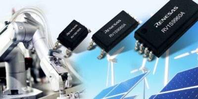
Three 15Mbits per second photocouplers from Renesas Electronics are designed to withstand the harsh operating environments of industrial and factory automation equipment. They have been developed in response to the trend for higher voltage, compact systems for safety standards and eco-friendly designs that require smaller ICs with lower power consumption. The RV1S9x60A family is claimed to have best-in-class low threshold input current (IFHL) ratings. The RV1S9160A (SO5) operates at 2.0mA, the RV1S9060A (LSO5) operates at 2.2mA and the RV1S9960A (LSDIP8) operates at 3.8mA.

Lower power consumption allows the RV1S9x60A photocouplers to suppress power supply heat generation. Operation at high temperatures, up to 125 degrees C (+110 degrees C for RV1S9960A) saves board space by allowing the photocoupler to be mounted near an IGBT or MOSFET power device. The devices are targeted at DC to AC power inverters, AC servo motors, programmable logic controllers (PLCs), robotic arms, solar and wind input power conditioners, and battery management systems for energy storage and charging.

The RV1S9x60A photocouplers feature high common mode rejection (noise tolerance) up to 50 kV/ micro seconds (minimum) to protect microcontrollers and other I/O logic circuits from high voltage spikes while transferring high-speed signals. The RV1S9x60A family also offers a variety of packages with the smallest footprint for each reinforced isolation (up to 690Vrms), and minimum creepage distances of 4.2 to 14.5mm to ensure safe operation.

The RV1S9160A, RV1S9060A and RV1S9960A photocouplers operate at low voltages, from 2.7 to 5.5V. Isolation voltages are 3,750Vrms (RV1S9160A), 5,000Vrms (RV1S9060A), and 7,500Vrms (RV1S9960A).

High temperature operation from -40°C to +125°C (RV1S9160A and RV1S9060A), and from -40°C to +110°C (RV1S9960A)

The supply current is 2.0mA (max), with a low pulse width distortion at 20 nanoseconds (max). Propagation delay is 60 nanoseconds max and propagation delay skew is 25 nanoseconds max.

The RV1S9x60A 15Mbits per second photocouplers are available now from Renesas Electronics’ worldwide distributors.

Renesas Electronics specialises in microcontrollers, analogue, power and SoC products for a range of automotive, industrial, home electronics, office automation, and information communication technology applications.

http://www.renesas.com

> Read More

ANPC inverter design secures ‘sweet spot’ for PV

According to Infineon Technologies, the use of an advanced neutral-point-clamped (ANPC) inverter design supports an even loss distribution between semiconductor devices, compared with traditional three-level neutral-point-clamped topologies. The company has used the ANPC topology for its hybrid SiC and IGBT power module EasyPack 2B in the 1,200V family. It is claimed to optimise ‘sweet spot’ losses of Infineon’s CoolSiC MOSFET and TrenchStop IGBT4 chipsets respectively, with increased power density and a switching frequency of up to 48kHz. The inverters are suitable for the needs of new generation 1,500V photovoltaic and energy storage applications, adds Infineon.

The ANPC topology supports a system efficiency of more than 99 per cent. Implementing the hybrid Easy 2B power module in, for example, the DC/AC stage of a 1,500V solar string inverter allows for coils to be smaller than with devices with a lower switching frequency. This reduces the weight “significantly” compared with a corresponding inverter with purely silicon components, says the company. Additionally, the losses with silicon carbide are smaller than with silicon. For this reason, less heat must be dissipated so that the heat sink can also shrink. This results in smaller inverter housings and costs savings at system level. The design also reduces inverter design complexity, compared to five-level topologies.

The Easy 2B standard package for power modules is characterised by an industry-leading low stray inductance. The integrated body diode of the CoolSiC MOSFET chip ensures low-loss without the need for another SiC diode chip. There is also an NTC temperature sensor for monitoring and PressFit technology to reduce assembly time for mounting the device.

The hybrid EasyPack 2B can be ordered now.

http://www.infineon.com

> Read More

Research indicates Pohoiki Beach chip for neural-inspired algortithms

An eight million neuron system, comprised of 64 Phokiki Beach chips, the codename for Loihi chips, is now available to the research community. The neuromorphic system will allow researchers to experiment with Lohi, Intel’s brain-inspired research chip, which applies the principles found in biological brains to computer architectures. Loihi enables users to process information up to 1,000 times faster and 10,000 times more efficiently than CPUs for specialised applications like sparse coding, graph search and constraint-satisfaction problems.

The early results success has led Intel to make Pohoiki Beach available to over 60 ecosystem partners, who will use the system to solve complex, compute-intensive problems, explained Rich Uhlig, managing director of Intel Labs.

Availability means researchers can now efficiently scale up neural-inspired algorithms — such as sparse coding, simultaneous localisation and mapping (SLAM), and path planning — that can learn and adapt based on data inputs.

Intel Labs hopes to scale the architecture to 100 million neurons later this year.

As new complex computing workloads become the norm, there is a growing need for specialised architectures designed for specific applications. This will be achieved by continued process node scaling in the same vein as the power-performance increases achieved by Moore’s Law.

Using the Pohoiki Beach neuromorphic system rather than general purpose computing technologies, Intel hopes to realise gains in speed and efficiency in autonomous vehicles, smart homes and cybersecurity.

“With the Loihi chip we’ve been able to demonstrate 109 times lower power consumption running a real-time deep learning benchmark, compared to a [graphics processor unit] GPU, and five times lower power consumption compared to specialised IoT inference hardware,” said Chris Eliasmith, co-CEO of Applied Brain Research and professor at University of Waterloo. He continued: “As we scale the network up by 50 times, Loihi maintains real-time performance results and uses only 30 per cent more power, whereas the IoT hardware uses 500 per cent more power and is no longer real-time.”

In another research project, Loihi has been used in a neural network that imitates the brain’s underlying neural representations and behaviour. “The SLAM solution emerged as a property of the network’s structure,” explained Konstantinos Michmizos of Rutgers University. “We benchmarked the Loihi-run network and found it to be equally accurate while consuming 100 times less energy than a widely used CPU-run SLAM method for mobile robots,” he said.

Later this year, Intel will introduce an even larger Loihi system, named Pohoiki Springs. Intel’s engineers expect that measurements from these research systems will quantify the gains that are achievable with neuromorphic-computing methods and will clarify the application areas most suitable for the technology. This research paves the way for the eventual commercialisation of neuromorphic technology.

The Intel’s Nahuku boards pictured each contain eight to 32 Intel Loihi neuromorphic chips, interfaced to an Intel Arria 10 FPGA development kit.

(Credit: Tim Herman/Intel Corporation)

http://www.intel.com

> Read More

Microchip adds FPGAs and IP to smart embedded vision initiative

Microchip has added low-power PolarFire FPGAs with enhanced high-speed imaging interfaces, an intellectual property (IP) bundle for image processing to its Smart Embedded Vision initiative.

FPGAs are increasingly popular in vision-based systems, for their high bandwidth processing capabilities in intelligent systems deployed in small form factors with tight thermal and power constraints.

The Smart Embedded Vision initiative provides a suite of FPGA offerings that includes IP, hardware and tools for low-power, small form factor machine vision designs across the industrial, medical, broadcast, automotive, aerospace and defence markets.

The initiative includes a serial digital interface (SDI) IP which is used to transport uncompressed video data streams over coaxial cabling. The interface is available in multiple speeds: HD-SDI (1.485Gbits per second, 720p, 1080i), 3G-SDI (2.970Gbits per second, 1080p60), 6G-SDI (5.94Gbits per second, 2Kp30) and 12G-SDI (11.88 Gbits per second, 2Kp60).

A MIPI-CSI-2 IP, operating at 1.5Gbits per second per lane is a sensor interface that links image sensors to FPGAs. The PolarFire family supports receive speeds up to 1.5Gbits per second per lane and transmit speeds up to 1Gbits per second per lane.

There is also an image sensor interface IP. The 2.3Gbits per second per lane SLVS-EC Rx – SLVS-EC Rx supports high-resolution cameras. Customers can implement a two-lane or eight-lane SLVS-EC Rx FPGA core.

Microsemi’sPolarFire family can support one, 2.5, five and 10Gbits per second speeds over an Ethernet PHY, enabling the initiative to meet the need for Universal Serial 10GE Media Independent Interface (USXGMII) MAC IP with auto-negotiation.

CoaXPress is a standard used in high- performance machine vision, medical and in industrial inspection. Microchip will support CoaXPress v2.0, which doubles the bandwidth to 12.5Gbits per second.

The HDMI 2.0b IP core today supports resolutions up to 4K at 60 frames per second transmit and 1080p at 60 frames per second receive.

The PolarFire FPGA imaging IP bundle features the MIPI-CSI-2 and includes image processing IPs for edge detection, alpha blending and image enhancement for colour, brightness and contrast adjustments.

A new ecosystem partner is Kaya Instruments, which provides PolarFire FPGA IP Cores for CoaXPress v2.0 and 10 GigE vision. The ecosystem also includes Alma Technology, Bitec and artificial intelligence partner ASIC Design Services, which provides a Core Deep Learning (CDL) framework that enables a power-efficient convolutional neural network (CNN)-based imaging and video platform for embedded and edge computing applications.

All Smart Embedded Vision solutions are supported by the Libero® SoC Design Suite, Microchip’s comprehensive development tool.

Through the Libero SoC Design Suite, all IP can be implemented on the PolarFire FPGA Video and Imaging Kit, the evaluation platform for Smart Embedded Vision designs.

http://www.microchip.com

> Read More

About Smart Cities

This news story is brought to you by smartcitieselectronics.com, the specialist site dedicated to delivering information about what’s new in the Smart City Electronics industry, with daily news updates, new products and industry news. To stay up-to-date, register to receive our weekly newsletters and keep yourself informed on the latest technology news and new products from around the globe. Simply click this link to register here: Smart Cities Registration