Holding out the promise for high-resolution applications in surveillance, biometric identification, virtual reality, research, and industrial automation, a thin-film monolithic image sensor developed by Imec captures light in the near-infrared (NIR) and short-wavelength infrared (SWIR).
Based on a monolithic approach, the process promises an order of magnitude gain in fabrication throughput and cost compared to processing today’s conventional infrared imagers, while enabling multi-megapixel resolution, claims Imec. It means that the use of infrared imagers can be extended to surveillance, biometric identification, virtual reality, machine vision and industrial automation.
Conventionally, infrared image sensors are produced through a hybrid technology of the crystalline semiconductor detector and the electronic readout fabricated separately and then interconnected at pixel or chip periphery level. This is an expensive and time-consuming process with low throughput. Sensors have a restricted resolution that often requires cooling to reduce the signal noise under dark conditions.
Imec’s infrared imagers consist of a novel thin-film photodetector pixel stack based on quantum dots deposited directly on top of an electronic readout. They are manufactured in a monolithic process compatible with wafer-based mass production, confirms Imec. The pixels embed newly developed high-performance, low bandgap, quantum dot materials that match or surpass the performance of inorganic light absorbers. The stacks can be tuned to target a spectrum from visible light up to two-micron wavelength. Test photodiodes on silicon substrate achieve an external quantum efficiency above 60 per cent at 940nm wavelength and above 20 per cent at 1450nm, allowing for uncooled operation with dark current comparable to commercial InGaAs photodetectors.
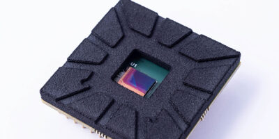
The prototype imager has a resolution of 758 x 512 pixels and five-micron pixel pitch.
“This result opens up many new applications for thin-film imagers,” commented Pawel Malinowski, imec’s thin-film imagers program manager. “Our imagers could be integrated in next-generation world-facing smartphone cameras coupled with eye-safe light sources, enabling compact sensing modules for augmented reality. In inspection, they could be used for food or plastics sorting, and in surveillance for low-light cameras with better contrast. Additionally, by enabling feature distinction in bad weather or smoke conditions, one can envision firefighting applications and, in the future, advanced driver assistance systems (ADAS),” he added.