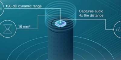
CrossLinkPlus FPGAs speed and enhance video bridging

Lattice Semiconductor has introduced the CrossLinkPlus FPGA family for MIPI D-PHY based embedded vision systems. The new devices are low power FPGAs featuring integrated flash memory, a hardened MIPI D-PHY and high-speed I/Os for instant-on panel display performance, and flexible on-device programming capabilities.

Developers want to enhance the user experience by adding multiple image sensors and/or displays to embedded vision systems, while also meeting system cost and power budgets.

Key features of the CrossLinkPlus family of FPGAs include on-device reprogrammable flash memory to enable instant-on (< 10 ms), hardened, pre-verified MIPI D-PHY interface supporting speeds up to 6 Gbps per port and broad support for high-speed I/O interfaces such as LVDS, SLVS and subLVDS.

Power consumption can be as low as 300 microwatt (standby) or 5 microwatt (operating).

Lattice also provides ready-to-use IPs and reference designs to accelerate implementation of enhanced sensor and display bridging, aggregation, and splitting functionality, a common requirement for industrial, automotive, computing, and consumer applications. There is a comprehensive IP library, including MIPI CSI-2, MIPI DSI, OpenLDI transmitters and receivers. These IPs are compatible with other Lattice FPGAs for easy design portability.

This new series is fully compatible with the Lattice Diamond design software tool flow, from synthesis and design capture through implementation, verification, and programming.

CrossLinkPlus uses its on-chip flash to support instant-on (minimising visual artifacts that detract from the user experience) and flexible device reprogramming in the field.

“The use of MIPI D-PHY in applications ranging from industrial control equipment displays to AI security cameras is booming as OEMs look to capitalize on the economies of scale driven by the MIPI ecosystem,” said Peiju Chiang, product marketing manager, Lattice Semiconductor.

“Lattice’s new CrossLinkPlus FPGAs combine the flexible programmability and speedy parallel processing of FPGAs with vision-specific hardware, software, pre-verified IPs and reference designs. This lets OEMs devote more time to building innovative applications and less time enabling standard functions that don’t offer any competitive differentiation.”

http://www.latticesemi.com

> Read More

Adaptable buck-boost converters deliver up to 2.5A in tiny packaging

A family of four high-efficiency, low-quiescent-current (IQ) buck-boost converters that feature tiny packaging with minimal external components for a small solution size is now available from Texas Instruments (TI).

The integrated TPS63802, TPS63805, TPS63806 and TPS63810 DC/DC non-inverting buck-boost converters offer wide input and output voltage ranges that scale to support multiple battery-driven applications, helping engineers simplify and accelerate their designs.

Each of the devices automatically selects buck, buck-boost or boost mode according to the operating conditions. Their complete solution size of 19.5 square mm to square mm 25 is a result of compact packaging, an advanced control topology requiring few external multilayer ceramic capacitors, and tiny 0.47-microH inductors.

The devices offer a 1.3-V to 5.5-V input and 1.8-V to 5.2-V output voltage range, to help engineers speed their designs and encourages reuse across multiple applications.

These DC/DC converters are the latest addition to TI’s low-IQ power-management portfolio, providing low 11- to 15-microA IQ for light-load efficiency while minimising power losses and extending run times in battery-driven applications such as portable electronic point-of-sale terminals, grid infrastructure metering devices, wireless sensors and handheld electronic devices.

The TPS63802 is a 2-A buck-boost converter with low 11-microA IQ consumption suitable for pulsed-load applications such as industrial Internet of Things devices. The TPS63805 is a 2-A buck-boost converter with a 22-microF output capacitor and 0.47-microH inductor resulting in a small solution size of 19.5 mm squared that meets the requirements of handheld industrial and personal electronics applications.

The new series also includes the TPS63806, a 2.5-A buck-boost converter with a focus on improved load-step regulation for applications with an aggressive load profile that require tight regulation, such as time-of-flight sensors in smartphones, cameras or augmented reality devices. And the

TPS63810 is a 2.5-A buck-boost converter with I2C interface for dynamic voltage scaling through either a two-wire interface or the VSEL pin, enabling the device to serve as a pre-regulator or voltage envelope tracker for systems found in smartphones, wireless hearing aids or headphones.

http://www.ti.com

> Read More

Automotive smart cameras use deep learning

Following a collaboration with, StradVision, Renesas Electronics announces the joint development of a deep learning-based object recognition solution for smart cameras. StradVision’s software has been optimised to run on Renesas Electronics’ R-Car SoCs.

The deep learning-based object recognition system is for smart cameras used in next-generation advanced driver assistance system (ADAS) applications and cameras for ADAS Level 2 and above.

Next-generation ADAS implementations require high-precision object recognition capable of detecting vulnerable road users (VRUs) such as pedestrians and cyclists. These systems must also consumer very low power for mass-market mid-tier to entry-level vehicles.

According to Naoki Yoshida, vice president of Automotive Technical Customer Engagement, at Renesas, StradVision is a leader in vision processing technology, with “abundant experience developing ADAS implementations using Renesas’ R-Car SoCs”. The collaboration has produced production-ready solutions “that enable safe and accurate mobility in the future,” said Yoshida. The deep learning based camera system is expected to contribute to the widespread adoption of next-generation ADAS implementations and support the escalating vision sensor requirements expected to arrive in the next few years.

StradVision’s deep learning–based object recognition software delivers high performance in recognising vehicles, pedestrians and lane marking. The high-precision recognition software has been optimised for Renesas R-Car automotive SoCs R-Car V3H and R-Car V3M. These R-Car devices incorporate a dedicated engine for deep learning processing called CNN-IP (Convolution Neural Network Intellectual Property), enabling them to run StradVision’s SVNet automotive deep learning network at high speed with minimal power consumption. The object recognition characteristic realises deep learning–based object recognition while maintaining low power consumption, suitable in mass-produced vehicles, encouraging ADAS adoption.

StradVision’s SVNet deep learning software is an AI perception solution for the mass production of ADAS systems. It is characterised by recognition precision in low-light environments and its ability to deal with occlusion when objects are partially hidden by other objects. The basic software package for the R-Car V3H performs simultaneous vehicles, person and lane recognition, processing the image data at a rate of 25 frames per second. Developers can customise the software, adding signs, markings and other objects as recognition targets. StradVision provides support for deep learning-based object recognition covering all the steps from training through the embedding of software for mass-produced vehicles.

In addition to the CNN-IP dedicated deep learning module, the Renesas R-Car V3H and R-Car V3M feature the IMP-X5 image recognition engine. The on-chip image signal processor (ISP) is designed to convert sensor signals for image rendering and recognition processing. This makes it possible to configure a system using inexpensive cameras without built-in ISPs, reducing the overall bill-of-materials (BoM) cost, says Renesas.

The R-Car SoCs featuring the new joint deep learning solution, including software and development support from StradVision, are scheduled to be available to developers by early 2020.

http://www.renesas.com

> Read More

IP with 112G Ethernet PHY targets hyperscale data centre SoCs

Enabling true long reach channels for 800G networking applications, Synopsys has introduced the DesignWare 112G Ethernet PHY on TSMC’s N7 process.

The DesignWare 112G Ethernet PHY IP on TSMC’s N7 process supports true long reach channels for up to 800G networking applications. It is based on Synopsys’ silicon-proven 56G Ethernet PHY available in multiple FinFET processes and delivers PAM-4 signalling for more than 35dB channel loss across optical, copper cables, and backplane interconnects.

The PHY’s transmit phase-locked loop architecture allows independent, per lane data rates for a broad range of high-throughput protocols and applications. To maximise bandwidth and beachfront density, the PHY’s layout allows square macros to be placed in a multi-row structure and along all edges of the die.

Synopsys offers a routing feasibility study, packages substrate guidelines, signal and power integrity models and thorough crosstalk analysis.

The 112G Ethernet PHY incorporates Synopsys’ data converters and implements power scaling techniques for up to 20 per cent power reduction in low-loss channels. Test features, including embedded bit-error rate tester and internal eye monitor, provide on-chip testability and visibility into channel performance. The 112G Ethernet PHY operates across voltage and temperature variations using continuous calibration and adaptation algorithms.

The DesignWare 112G Ethernet PHY for TSMC’s N7 process is scheduled to be available in Q1 of 2020.

DesignWare IP from IP for SoC designs provider, Synopsys, includes logic libraries, embedded memories, embedded test, analogue IP, wired and wireless interface IP, security IP, embedded processors, and subsystems. To accelerate prototyping, software development, and integration of IP into SoCs, Synopsys’ IP Accelerated initiative offers IP prototyping kits, IP software development kits, and IP subsystems.

Synopsys is the Silicon to Software partner for companies developing electronic products and software applications. The company has a long history in electronic design automation (EDA) and semiconductor IP and is also growing its leadership in software security and quality solutions. Customers are SoC designers creating advanced semiconductors, or a software developer writing applications that require high security and quality.

http://www.synopsys.com

> Read More

About Smart Cities

This news story is brought to you by smartcitieselectronics.com, the specialist site dedicated to delivering information about what’s new in the Smart City Electronics industry, with daily news updates, new products and industry news. To stay up-to-date, register to receive our weekly newsletters and keep yourself informed on the latest technology news and new products from around the globe. Simply click this link to register here: Smart Cities Registration