Designed to support base station applications (including single and multi-standard 3G/4G/5G macrocell base stations, massive multiple input multiple output (M-MIMO), and small cell systems, the ADRV9026 is the latest member of Analog Devices’ RadioVerse family.
The quad-channel, wideband RF transceiver offers quad-channel integration with the lowest power, smallest size, common-platform solution, according to Analog Devices.
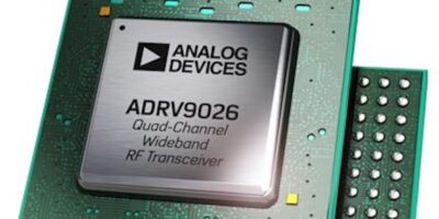
It is supplied in a 14 x 14mm BGA package and is claimed to be the smallest size, lowest power transceiver for base transceiver stations. The small size reduces footprint and enhances form factor flexibility.
It also reduces power consumption by 50% compared with the previous generation, ADVR9009, for increased radio density and enables open radio access network (ORAN) small cell designs with lowest system power and cost, the company continued.
The integrated, high performance software defined radio supports up to 200MHz bandwidth and covers all bands from 650MHz to 6GHz.
Other features are the quad-channel transmitters and receivers with dual-channel observation receivers, local oscillator (LO) frequency of 650 to 6,000MHz and a maximum receiver/transmitter bandwidth of 200MHz. Maximum observation receiver/transmitter synthesis bandwidth is 450MHz.
There is also multi-chip phase synchronisation for all local oscillators and baseband clocks.
Future software upgrades for new features will include external local oscillator support, extending the local oscillator frequency down to 75MHz, with Filter Wizard to support custom profiles.
A common platform design for 3G, 4G and 5G reduces complexity, development costs and time to market, says Analog Devices. The single-chip FDD/TDD simplifies hardware and software development and a common application programming interface addresses multiple applications.
For macro base stations or small cell designs the ADVR9009 reduces product development cycles for band and power variants and enables modular architecture for scalable radio solutions. An evaluation kit is also available.