Power semiconductors from Renesas and timing solutions from its subsidiary, IDT, support the Xilinx Versal adaptive compute acceleration platform (ACAP) devices featured on the Xilinx VCK190 evaluation kit and the Renesas VERSALDEMO1Z power reference board.
The 7nm process Versal is the industry’s first ACAP platform that addresses applications in data centre, automotive, 5G wireless, and wired and defence markets, says Renesas.
The company provides turnkey clocking and power reference boards that help system developers jumpstart Versal ACAP designs. For developers creating complex, compute-intensive systems that demand flexible and high-performance power delivery and timing, the collaboration has resulted in pre-validated reference designs that allow developers to rapidly develop and optimise system performance and power efficiency.
The Xilinx VCK190 is the first Versal AI Core series evaluation kit. It is based on the VC1902 Versal AI Core series ACAP, providing AI inference and signal processing throughput for cloud, network, and edge applications. The kit features complete timing solutions including the 8A34001 ClockMatrix system synchroniser for IEEE1588 and eCPRI applications, 8T49N240/8T49N241 Universal Frequency Translators for low-jitter and flexible transceiver SerDes clocking, a programmable clock generator and clock buffer/multiplexer for PCIe interface.
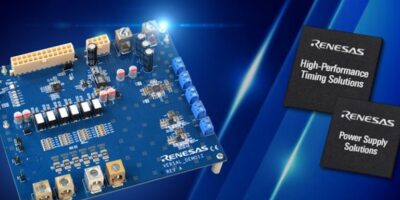
The Renesas VERSALDEMO1Z power reference board provides full power rails for the Versal ACAP’s adaptable engines, AI engines, scalar engines, and external DDR memory. The board is a complete power supply solution featuring one member of the ISL68xxx digital multiphase PWM controller family and multiple members of the ISL99xxx smart power stage family to provide high-efficiency and scalable Vcore power. There are also ISL91211A power management IC (PMIC) and DC/DC regulators.
The Renesas VERSALDEMO1Z power reference board is available now from Renesas Electronics.
Renesas Electronics delivers semiconductors that enable billions of connected, intelligent devices, microcontrollers, analogue, power, and SoC products for automotive, industrial, home electronics, office automation, and information communication technology applications.