Software accelerates AI deployment in audio, voice and sensing devices

Software for Cadence Tensilica HiFi digital signal processors (DSPs) has been optimised to execute TensorFlow Lite for Microcontrollers, part of the TensorFlow open-source platform for machine learning (ML) from Google. The edge-based ML running on the low power cores supports intelligence in audio, voice and sensing applications.

The HiFi DSPs are the first DSPs to support TensorFlow Lite for Microcontrollers, says Cadence. The software support for TensorFlow Lite on the HiFi DSP cores, promotes development of edge applications that use artificial intelligence (AI) and ML on TensorFlow and removes the need for hand-coding neural networks. This accelerates time to market, Cadence notes.

Implementing AI at the edge on devices that use voice and audio as a user interface, requires the inference model to be run on the device. This eliminates the latency associated with sending data to a cloud service and waiting for the response to be sent back to the device and also reduces power consumption associated with sending/receiving large amounts of data across a network.

It also serves to maintain privacy and minimise security issues since the data does not leave the device. As the device is not dependent on the cloud, it can be disconnected from the network and still operate.

A 600MHz Tensilica HiFi 4 DSP is included in NXP Semiconductor’s i.MX RT600 and delivers 4.8 Giga multiply-accumulates per second (GMACS). It has the compute power required for deploying voice, audio and other neural network-based applications at the edge. Joe Yu, vice president of microcontrollers at NXP Semiconductors, said: “Supporting the popular, end-to-end toolchain, TensorFlow, as well as other inferencing technologies, on the HiFi DSP will enable ML developers to take advantage of the compelling combination of compute and memory on this chip”.

Yipeng Liu, director of audio/voice IP at Cadence, added: “Support for TensorFlow Lite for Microcontrollers enables our licensees to innovate with ML applications like keyword detection, audio scene detection, noise reduction and voice recognition, with the assurance that they can run in an extremely low-power footprint”.

http://www.cadence.com

> Read More

Wideband mmWave synthesiser is for 5G radio beamforming and MIMO

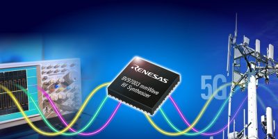
The integrated 8V97003 wideband mmWave synthesiser is has the industry’s highest performance and features optimised for 5G and broadband wireless applications, says Renesas Electronics.

The 8V97003 can be used as a local oscillator (LO) for mmWave and beamforming, or a precision reference clock for a high-speed data converter in test and measurement, optical networking and data acquisition applications.

According to Bobby Matinpour, vice president of Timing Products, IoT and Infrastructure business unit at Renesas: “[The] single-chip . . .  8V97003 is particularly well-suited for emerging applications above the 6GHz carrier frequency, including broadband wireless, microwave backhaul, and 5G radios”.

The 8V97003 is claimed to deliver the industry’s best combination of wide frequency range (171.875MHz to 18GHz), low output phase noise (-60.6dBc at 20kHz to 100MHz at 6GHz) and high output power over its entire frequency range. Engineers can use a single 8V97003 in place of multiple synthesiser modules to reduce footprint and cost of the end product. The high output power eliminates the need for external driver which reduces complexity and power consumption without compromising performances, says Renesas. The low output phase noise makes it suitable for 5G and other wireless applications where it is claimed to enable superior system level signal-to-noise ratio (SNR) and error vector magnitude (EVM). As a reference clock for high-speed data converters, the 8V97003 maximises system performance by improving SNR and spurious-free-dynamic-range (SFDR).

Mass production quantities of the 8V97003 are available now in a 7.0 x 7.0mm, 48-lead VFQFPN package.

http://www.renesas.com

> Read More

Infineon and Qualcomm enable standard solution for 3D authentication

A reference design developed by Infineon Technologies, working with Qualcomm Technologies is for 3D authentication based on the Qualcomm Snapdragon 865 mobile platform.

The reference design uses the REAL3 3D time of flight (ToF) sensor and enables a standardised integration for smartphone manufacturers.

At CES 2020, Infineon introduced the 4.4 x 5.1mm ToF sensor, describing it as the world’s smallest yet most powerful 3D image sensor with VGA resolution. It can be used for face authentication, enhanced photo features and authentic augmented

Andreas Urschitz, division president power management and multimarket at Infineon, commented: “3D sensors enable new uses and additional applications such as secured authentication or payment by facial recognition. We continue to focus on this market and have clear growth targets”.

Infineon develops the 3D ToF sensor technology in co-operation with the software and 3D time-of-flight system specialist pmdtechnologies.

From this month, Infineon’s REAL3 ToF sensor will enable the video bokeh function for the first time in a 5G-capable smartphone for optimal image effects even in moving images. Using the precise 3D point cloud algorithm and software, the received 3D image data is processed for the application. The 3D image sensor captures 940nm infrared light reflected from the user and the scanned objects. It also uses high-level data processing to achieve accurate depth measurements. The patented SBI (Suppression of Background Illumination) technology offers a wide dynamic measuring range from bright sunlight to dimly lit rooms for robust operation without loss of data processing quality.

pmdtechnologies is a fabless IC company headquartered in Siegen, Dresden and Ulm with subsidiaries in the USA, China and Korea. It claims to be the leading 3D ToF CMOS-based digital imaging technology supplier. Founded in 2002, the company owns over 350 worldwide patents concerning pmd-based applications, the pmd measurement principle and its realisation. The company operates in industrial applications.

http://www.infineon.com

> Read More

Lattice supports embedded vision with solutions stack

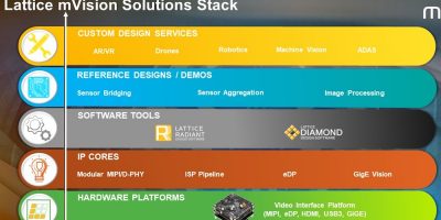
To accelerate low power, embedded vision development such as image sensor bridging, aggregation, splitting and processing, Lattice Semiconductor has introduced the mVision solutions stack with support for the Nexus platform and CrossLink-NX FPGAs.

It includes the modular hardware development boards, design software, embedded vision IP portfolio, reference designs and demos needed to implement sensor bridging, sensor aggregation, and image processing applications found in machine vision, advanced driver assistance systems (ADAS), drones and augmented reality / virtual reality (AR/VR) for the industrial, automotive, consumer, smart home and medical markets.

Initially used in manufacturing, today embedded vision is used in automated assembly and inventory, explained Jeff Bier, founder of the Edge AI and Vision Alliance. “Many of these applications demand small, low cost, low power solutions,” he continued, adding “Solutions stacks, such as sensAI and mVision . . . help developers more easily integrate smart vision capabilities into their product designs.”

Key features of the Lattice mVision solutions stack are the Video Interface Platform (VIP) modular hardware development boards with support for a variety of video and I/O interfaces commonly used in embedded vision applications (including MIPI, LVDS, DisplayPort, HDMI, USB, and others). The VIP development boards currently support Lattice FPGAs including CrossLink, ECP5 and CrossLink-NX, based on the Lattice Nexus platform.

There is also a comprehensive IP Library. The Lattice mVision solutions stack includes ready-to-implement IP cores for interfacing to MIPI and LVDS image sensors, image signal processing pipelines, common connectivity standards like USB and Gigabit Ethernet, and display standards such as HDMI, DisplayPort, and GigE Vision.

The stack supports both of Lattice’s FPGA design tools, Lattice Diamond and Lattice Radiant. The tools automate many common design tasks.

There are also complete reference designs for common embedded vision applications including sensor bridging, sensor aggregation and image processing.

Customers can also access a  network of design service partners, developed by Lattice, for support ranging from developing individual functional design blocks to complete turn-key solutions.

http://www.latticesemi.com/mvision

> Read More

About Smart Cities

This news story is brought to you by smartcitieselectronics.com, the specialist site dedicated to delivering information about what’s new in the Smart City Electronics industry, with daily news updates, new products and industry news. To stay up-to-date, register to receive our weekly newsletters and keep yourself informed on the latest technology news and new products from around the globe. Simply click this link to register here: Smart Cities Registration