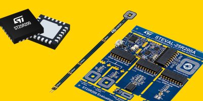
ST is making it easier to explore creative applications for contactless near-field communication (NFC) technology with a novel development kit featuring the new ST25R200 reader/writer IC. ST’s latest-generation ST25R200 NFC transceiver combines an advanced design for strong and clear wireless connections with low power consumption and controls for signal quality and power management.
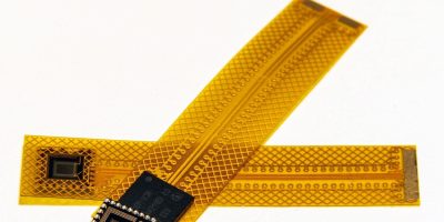
The STEVAL-25R200SA kit for reader evaluation contains an ultra-compact ST25R200 board, ready for power-up, and multiple antennas that let users try single, dual, and flexible designs. The evaluation kit is complete with a 50-Ohm antenna interface and programmable tags.
This modular kit helps quickly build proof-of-concept models to demonstrate convenient short-range wireless communications for device pairing, configuring settings, or product authentication to ensure brand protection. The main board and antennas are NFC-certified and suitable for diverse industrial, consumer, and health technologies, such as medical devices, power tools, household appliances, game consoles, and personal care devices.
The ST25R200 NFC reader features ST’s noise suppression receiver (NSR), which ensures high immunity to interference even when close to a noise source such as an LCD panel contained in the same device. The receive circuitry also features an advanced analog front end (AFE), standard NFC-A/B (ISO 14443A/B) and NFC-V (ISO 15693) data framing.
Enhanced low-power card detection (LPCD), also built-in, eases wake-up to ensure a smooth and seamless user experience. The 1.2W transmitter has dynamic power output (DPO) control to regulate the field strength and overshoot/undershoot protection to ensure consistent signalling throughout data exchanges.
This reader operates over a wide power supply and peripheral I/O voltage range from 2.7V to 5.5V and from -40°C to 85°C. In addition, there are multiple operating modes to assist power management, cutting the device current to as little as 1µA to extend the runtime of battery-powered applications. In reset mode the IC draws just 0.1µA.