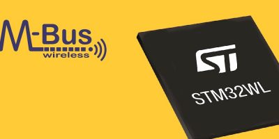
Wideband mmWave synthesiser is for 5G radio beamforming and MIMO

The integrated 8V97003 wideband mmWave synthesiser is has the industry’s highest performance and features optimised for 5G and broadband wireless applications, says Renesas Electronics.

The 8V97003 can be used as a local oscillator (LO) for mmWave and beamforming, or a precision reference clock for a high-speed data converter in test and measurement, optical networking and data acquisition applications.

According to Bobby Matinpour, vice president of Timing Products, IoT and Infrastructure business unit at Renesas: “[The] single-chip . . .  8V97003 is particularly well-suited for emerging applications above the 6GHz carrier frequency, including broadband wireless, microwave backhaul, and 5G radios”.

The 8V97003 is claimed to deliver the industry’s best combination of wide frequency range (171.875MHz to 18GHz), low output phase noise (-60.6dBc at 20kHz to 100MHz at 6GHz) and high output power over its entire frequency range. Engineers can use a single 8V97003 in place of multiple synthesiser modules to reduce footprint and cost of the end product. The high output power eliminates the need for external driver which reduces complexity and power consumption without compromising performances, says Renesas. The low output phase noise makes it suitable for 5G and other wireless applications where it is claimed to enable superior system level signal-to-noise ratio (SNR) and error vector magnitude (EVM). As a reference clock for high-speed data converters, the 8V97003 maximises system performance by improving SNR and spurious-free-dynamic-range (SFDR).

Mass production quantities of the 8V97003 are available now in a 7.0 x 7.0mm, 48-lead VFQFPN package.

http://www.renesas.com

> Read More

Infineon and Qualcomm enable standard solution for 3D authentication

A reference design developed by Infineon Technologies, working with Qualcomm Technologies is for 3D authentication based on the Qualcomm Snapdragon 865 mobile platform.

The reference design uses the REAL3 3D time of flight (ToF) sensor and enables a standardised integration for smartphone manufacturers.

At CES 2020, Infineon introduced the 4.4 x 5.1mm ToF sensor, describing it as the world’s smallest yet most powerful 3D image sensor with VGA resolution. It can be used for face authentication, enhanced photo features and authentic augmented

Andreas Urschitz, division president power management and multimarket at Infineon, commented: “3D sensors enable new uses and additional applications such as secured authentication or payment by facial recognition. We continue to focus on this market and have clear growth targets”.

Infineon develops the 3D ToF sensor technology in co-operation with the software and 3D time-of-flight system specialist pmdtechnologies.

From this month, Infineon’s REAL3 ToF sensor will enable the video bokeh function for the first time in a 5G-capable smartphone for optimal image effects even in moving images. Using the precise 3D point cloud algorithm and software, the received 3D image data is processed for the application. The 3D image sensor captures 940nm infrared light reflected from the user and the scanned objects. It also uses high-level data processing to achieve accurate depth measurements. The patented SBI (Suppression of Background Illumination) technology offers a wide dynamic measuring range from bright sunlight to dimly lit rooms for robust operation without loss of data processing quality.

pmdtechnologies is a fabless IC company headquartered in Siegen, Dresden and Ulm with subsidiaries in the USA, China and Korea. It claims to be the leading 3D ToF CMOS-based digital imaging technology supplier. Founded in 2002, the company owns over 350 worldwide patents concerning pmd-based applications, the pmd measurement principle and its realisation. The company operates in industrial applications.

http://www.infineon.com

> Read More

Lattice supports embedded vision with solutions stack

To accelerate low power, embedded vision development such as image sensor bridging, aggregation, splitting and processing, Lattice Semiconductor has introduced the mVision solutions stack with support for the Nexus platform and CrossLink-NX FPGAs.

It includes the modular hardware development boards, design software, embedded vision IP portfolio, reference designs and demos needed to implement sensor bridging, sensor aggregation, and image processing applications found in machine vision, advanced driver assistance systems (ADAS), drones and augmented reality / virtual reality (AR/VR) for the industrial, automotive, consumer, smart home and medical markets.

Initially used in manufacturing, today embedded vision is used in automated assembly and inventory, explained Jeff Bier, founder of the Edge AI and Vision Alliance. “Many of these applications demand small, low cost, low power solutions,” he continued, adding “Solutions stacks, such as sensAI and mVision . . . help developers more easily integrate smart vision capabilities into their product designs.”

Key features of the Lattice mVision solutions stack are the Video Interface Platform (VIP) modular hardware development boards with support for a variety of video and I/O interfaces commonly used in embedded vision applications (including MIPI, LVDS, DisplayPort, HDMI, USB, and others). The VIP development boards currently support Lattice FPGAs including CrossLink, ECP5 and CrossLink-NX, based on the Lattice Nexus platform.

There is also a comprehensive IP Library. The Lattice mVision solutions stack includes ready-to-implement IP cores for interfacing to MIPI and LVDS image sensors, image signal processing pipelines, common connectivity standards like USB and Gigabit Ethernet, and display standards such as HDMI, DisplayPort, and GigE Vision.

The stack supports both of Lattice’s FPGA design tools, Lattice Diamond and Lattice Radiant. The tools automate many common design tasks.

There are also complete reference designs for common embedded vision applications including sensor bridging, sensor aggregation and image processing.

Customers can also access a  network of design service partners, developed by Lattice, for support ranging from developing individual functional design blocks to complete turn-key solutions.

http://www.latticesemi.com/mvision

> Read More

Microcontroller with built-in PUF tech offers multiple layers of security

The MAX32520 ChipDNATM secure Arm Cortex-M4 microcontroller from Maxim Integrated Products is a secure microcontroller with built-in physically unclonable function (PUF) technology for financial- and government-grade security. The technology allows for multiple layers of protection to provide advanced key-protection technology for use in Internet of Things (IoT), health care, industrial and computing systems.

The MAX32520 with ChipDNA offers multiple layers of protection through its PUF technology, a key-protection technology for safeguarding secrets used in cryptographic operations. It uses a tamper-proof PUF key for flash encryption, secure boot for root-of-trust and serial flash emulation. Additionally, the physical security inherent in the PUF key eliminates the need for a battery to actively destroy secret-key materials when under attack. Until now, the most-sensitive applications have always required a battery to provide this highest level of secret-key protection.

The secret keys generated by the ChipDNA PUF circuitry are resistant to physical attacks, ensuring the keys that protect data and systems are out of the reach of attackers. Flash-encryption using PUF protects sensitive information with encryption keys that can withstand advanced physical inspection and prying, as well as providing robust IP security. The DeepCover secure microcontroller can protect all user data, as it is equipped with SP 800-90A and SP 800-90B compliant TRNG and hardware accelerators for AES-256, ECDSA P-521 and SHA-512.

Delivering up to 2MB of secure flash memory means advanced applications can run in a highly secure environment. Built on an advanced process node, this secure microcontroller provides advanced security features, a 120 MHz ARM Cortex M4 processor and plenty of memory. It eliminates several components like a battery, a tamper monitor IC and system management micros that are often found in security-sensitive applications.

“Enabling developers to incorporate PUF-encrypted flash and secure boot loading without system redesign or in-house code development will help them reduce time-to-market dramatically,” said Tanner Johnson, senior analyst, IoT cybersecurity at Omdia.

Kris Ardis, executive director, micros, security and software business unit at Maxim Integrated said: “The threats to IoT systems are getting more advanced all the time, and tools to attack systems move from the realm of academia to the realm of open source every day. MAX32520 with ChipDNA is a step forward.”

http://www.maximintegrated.com

> Read More

About Smart Cities

This news story is brought to you by smartcitieselectronics.com, the specialist site dedicated to delivering information about what’s new in the Smart City Electronics industry, with daily news updates, new products and industry news. To stay up-to-date, register to receive our weekly newsletters and keep yourself informed on the latest technology news and new products from around the globe. Simply click this link to register here: Smart Cities Registration