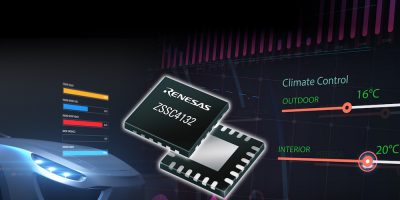
NXP offers Wi-Fi 6 processors for automotive and IoT

Wi-Fi 6 (802.11ax) devices from NXP Semiconductors support developers’ efforts to adopt the latest Wi-Fi standards. The company says its expanded Wi-Fi 6 portfolio applies to connectivity for automotive, access, mobile and industrial and IoT markets.

Wi-Fi 6 delivers symmetric multi-gigabit uploads and downloads, lower latency, increased capacity and improved power efficiency, explains NXP. These technical advancements have so far been limited to premium products but NXP says these benefits are now available for large-scale deployment across multiple markets, enabling products with up to four-fold performance improvement, greater range, improved battery life and greater connection reliability for Wi-Fi capabilities. Wi-Fi 6 connectivity can be applied to smart homes, connected cars, and industrial machinery.

The portfolio consists of the 88W9064 and 88W9068, 4×4 and 8×8-stream solutions with integrated Bluetooth 5 for home and enterprise access solutions, the 88Q9098 concurrent dual Wi-Fi 2×2+2×2 + Bluetooth 5 AEC-Q100-qualified devices for infotainment and telematics automotive applications, the 88W9098, concurrent dual Wi-Fi 2×2+2×2 + Bluetooth 5 devices for multimedia streaming and consumer access applications. Others are IoT-focused 2×2 WiFi 6 + Bluetooth 5 devices.

NXP’s RF front-end solutions are based on silicon germanium (SiGe) and can scale Wi-Fi 6 capabilities from low to high-end applications, including 1×1, 2×2, 4×4 and 8×8 multiple input, multiple output (MIMO). It is packaged in a compact 3.0 x 4.0mm module for mobile products.

“To date, the adoption of Wi-Fi 6 has predominantly been driven by smartphones. However, we expect significant traction to build within the IoT, infrastructure, and automotive markets throughout 2020 and beyond. said Andrew Zignani, Wi-Fi, Bluetooth, and Wireless Connectivity Principal Analyst at ABI Research.

When combined with the processing power of the EdgeVerse platform, NXP enables smart connected devices, connecting people to the internet, joining IoT devices to the cloud, or communicating with cars.

NXP Semiconductors says it is the world leader in secure connectivity solutions for embedded applications, and is driving innovation in the automotive, industrial and IoT, mobile, and communication infrastructure markets. It has more than 60 years of combined experience and expertise, with employees in more than 30 countries.

http://www.nxp.com

> Read More

IO-Link IC connects industry 4.0 devices

The CCE4503 is the latest member of the IO-Link family from Dialog Semiconductor.  It is the first to be launched by the company since it bought Creative Chips at the end of last year. The IC connects the smallest and most price-sensitive IO-Link device sensors and actuators for the industrial IoT (IIoT).

IO-Link is the first globally standardised, serial bi-directional point-to-point communication technology (IEC 61131-9) for an industrial automation network, providing data access to the cloud. It provides robust communications for the last stretch between sensors, actuators and any fieldbus within a network.

The CCE4503 is a robust device-side IO-Link-compliant transceiver that combines IO-Link standard communications with advanced protection circuitry and low power dissipation. It is packaged in a tiny DFN10 (3.0 x 3.0mm). Its size enables it to be used to add IO-Link connectivity to the most space-constricted industrial sensor and actuator devices, says Dialog.

“Industrial sensors and actuators are integrating more functionality in smaller form factors with greater demands for cloud connectivity,” said Dr Lutz Porombka, vice president of Dialog’s Industrial Mixed Signal business unit.

The CCE4503 is sampling now and is supported by a comprehensive set of development support tools, industry standard IO-Link software and a full-featured customer evaluation board.

https://www.dialog-semiconductor.com

> Read More

Image sensors for computer vision use ST’s die-stacking technology

Two high-speed image sensors released by STMicroelectronics use global shutter to capture images. Global shutter mode captures distortion-free images when the scene is moving or when near-infrared illumination is needed. This makes the sensors suitable for use in the next generation of smart computer vision applications, says ST.

Global-shutter sensors save all pixel data in each frame simultaneously, contrasting with rolling-shutter operation that captures pixel data sequentially, which makes moving images vulnerable to distortion or in need of additional corrective processing.

The company’s image sensor process technologies are claimed to enable class-leading pixel size while offering both high sensitivity and low crosstalk. The silicon process innovation and advanced pixel architecture allows a smaller sensor pixel array on the top die, while keeping more silicon area on the bottom die to increase digital-processing capabilities and features.

ST’s advanced pixel technology, including full deep trench isolation (DTI), enables extremely small 2.61 x 2.61 micron pixels that combine low parasitic light sensitivity (PLS), high quantum efficiency (QE), and low crosstalk in a single die layer.

The VD55GO sensor has 640 x 600 pixels and the VD56G3 sensor has 1.5Mpixels (1124 x 1364). The VD55GO measures 2.6 x 2.5mm and the VD56G3 measures 3.6mm x 4.3mm, making them the smallest image sensors available today, in relation to resolution, says ST.

They also have low pixel-to-pixel crosstalk at all wavelengths, specifically near-infrared, which ensures high contrast for image clarity. Embedded optical-flow processing in the VD56G3 calculates movement vectors, without the need for host computer processing.

The sensors are intended for a wide range of applications including augmented reality / virtual reality (AR/VR), simultaneous localisation and mapping (SLAM), and 3D scanning.

According to Eric Aussedat, imaging sub-group general manager and executive vice president of the Analog, MEMS and Sensors Group, STMicroelectronics: “They are enabling another step forward in computer-vision applications, empowering designers to create tomorrow’s smart, autonomous industrial and consumer devices.”

Samples are shipping now to lead customers.

http://www.st.com

> Read More

nRF52820 SoC is introduced to support lower-end of nRF52 series     

The nRF52820 Bluetooth 5.2 SoC is the sixth addition to Nordic Semiconductor’s nRF52 Series. It is a low power Bluetooth Low Energy (Bluetooth LE), Bluetooth mesh, Thread, Zigbee, and 2.4GHz proprietary wireless connectivity device for smart home, commercial and industrial applications.

The nRF52820’s is capable of all the features of Bluetooth 5, 5.1 and 5.2 including long range and high-throughput of 2Mbits per second, as well as direction finding, low energy power control and low energy isochronous channels.

It has a full speed (12Mbits per second) USB 2.0 interface. The USB connectivity interface enables low-latency and high-bandwidth communication with a range of host devices, such as PCs, smartphones, and gateways. The connectivity also makes device firmware updates (DFU)-over-USB practical. In addition to the main supply regulators, the USB peripheral in the nRF52820 includes a dedicated regulator for converting the 5V Vbus signal to the 3.3V needed for the USB signalling interface, which negates the need for an external regulator, saving both cost and space.

Based on a 64MHz 32bit Arm Cortex-M4 processor, the SoC includes 256kbyte Flash and 32kbyte RAM. This, says Nordic, makes it particularly well-suited as a single-chip option for commercial and industrial wireless applications including professional lighting, asset tracking, high intensity discharge lighting and gaming products.

When paired with an application microcontroller, the nRF52820’s multi-protocol radio and +8dBm output power enables its use as a network processor for gateways and other smart home applications that require advanced wireless connectivity.

The nRF52820 is qualified for operation across an extended industrial temperature range of -40 to 105 degrees C.

The nRF52820 includes up to 18 general purpose I/Os and a range of analogue and digital interfaces such an analogue comparator, SPI, UART, TWI, and QDEC.

The supply voltage covers a 1.7 to 5.5V input range, allowing the nRF52820 to be powered by coin-cells and rechargeable batteries.

The nRF52820 is supported by the S112 and S140 SoftDevices (Bluetooth 5.1-qualified protocol stacks), and the S122 (alpha version) SoftDevice. The S112 and S122 are memory-optimised peripheral and central stacks respectively, while the S140 is a feature-complete Bluetooth 5 protocol stack for central and peripheral, including long range and high-throughput.

Nordic also offers the nRF5 software development kit (SDK) v16.0.0, with the full nRF5 SDK support to follow in Q2 2020. The nRF52833 development kit can be used to emulate the nRF52820 and as a basis to start nRF52820-based designs.

http://www.nordicsemi.com

> Read More

About Smart Cities

This news story is brought to you by smartcitieselectronics.com, the specialist site dedicated to delivering information about what’s new in the Smart City Electronics industry, with daily news updates, new products and industry news. To stay up-to-date, register to receive our weekly newsletters and keep yourself informed on the latest technology news and new products from around the globe. Simply click this link to register here: Smart Cities Registration