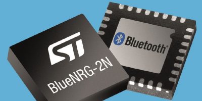
Dialog Semiconductor combines Wi-Fi and BLE in DA16600 modules

Leveraging the DA16200 VirtualZero Wi-Fi technology with SmartBond Tiny DA14531 Bluetooth, Dialog Semiconductor claims that the DA16600 module offers best-in-class battery life and configurability.

The DA16200 SoC was purpose-built for battery-powered IoT applications, including connected door locks, thermostats, security cameras and other devices that require an always-on Wi-Fi connection, but may be only used sporadically. Its VirtualZero technology enables the industry’s lowest level of power consumption for Wi-Fi connectivity, so that even continuously connected devices can achieve up to five years of battery life in many use cases, said Dialog Semiconductor. The DA16600 module also leverages the capabilities of the SmartBond TINY DA14531, claimed to be the world’s smallest and lowest power Bluetooth SoC.

The DA16600 Wi-Fi and Bluetooth Low Energy module combines the two complex protocol stacks, eliminating issues often caused by the co-existence of two radios at 2.4GHz in the same design, said Dialog. Bluetooth Low Energy provides ease of configurability for Wi-Fi in the application, simplifying the task of Wi-Fi set up for the end user. The module design is optimised to be incorporated into an embedded IoT product using is a simple set of guidelines provided by Dialog.

The module is certified for worldwide operation, including certifications for FCC, IC, CE, Telec, Korea and SRRC. It is also Wi-Fi Certified for interoperability.

Evaluation boards and a complete software development kit (SDK) are available for the DA16600 module via DigiKey. The SDK includes sample applications, provisioning apps, AT command library and power management tools.

https://www.dialog-semiconductor.com

> Read More

NFC reader IC delivers rapid car key response and extended range

STMicroelectronics says the latest addition to the ST25R NFC reader ICs deliver rapid car-key response and reliable connections over extended distances. The ST25R3920 complies to the recently published Digital Key Release 2.0 specification by the Car Connectivity Consortium and certified by NFC Forum.

Digital keys let drivers conveniently lock and unlock their cars using smartphones, and support added-value features including easy sharing and management of access privileges for other users. The keys could also enable new vehicle-ownership models, including car subscription services.

The Car Connectivity Consortium (CCC) Digital Key Release 2.0, relaying on NFC, offers the ability to use the key while the phone battery is so low that normal device operation is disabled.

The ST25R3920 uses Dynamic Power Output (DPO) and Noise-Suppression Receiver (NSR) technologies to increases RF output power and enhance input-circuit design for rapid car-key response, said STMicroelectronics.

With DPO, the device operates at up to 1.6W continuous RF output power and 2.5W short-term input peak, to maintain reliable NFC connections over distance with a small antenna. ST’s NSR technology increases immunity to interference from noise sources to simplify EMI and is also claimed to ease certification. Automatic antenna tuning compensates for changes in the RF environment to maintain the best possible connection to the user’s smartphone, while low-power key-signal detection with inductive wakeup minimises load on the battery when the key is not being used.

The ST25R3920 has been designed for space-constrained locations that severely limit the maximum antenna size, as a result in can be positioned in door handles, B-pillar, or centre console.

 The ST25R3920 supports the CCC Digital Key Standardization Release 2.0, the architecture endorsed by the world’s leading carmakers, smartphone manufacturers, and electronics suppliers. ST is a CCC member and plays a key role in setting NFC standards as a member of the NFC Forum board, various working groups, and ISO 14443 and ISO 15693 task forces.

The IC is also certified by NFC Forum and can work as an NFC reader or NFC universal device. Compliance with NFC Forum standards for pairing applications, as well as EMVCo 3.0 standards, allows its use as an in-car contactless-payment terminal for services such as electric-vehicle charging. In addition, a Qi wireless charging NFC-card protection algorithm enables safe wireless charging of portable devices.

The ST25R3920 is in production now.

http://www.st.com

> Read More

AI stack doubles performance for edge AI

For on-device AI processing at the edge, Lattice Semiconductor has introduced the sensAI 3.0, available on low power, 28nm FD-SOI-based Lattice CrossLink-NX FPGAs.

This latest version of the company’s stack features customised convolutional neural network (CNN) IP. This flexible accelerator IP simplifies the implementation of common CNN networks, explained Lattice, and is optimised to leverage the parallel processing capabilities of FPGAs. Adding support for CrossLink-NX FPGAs brings new levels of power and performance to smart vision applications in the surveillance/security, robotics, automotive and computing markets, said the company.

To address data security, latency and privacy issues, developers want to move the AI processing that powers their smart vision and other AI applications from the cloud to the edge. Most edge devices are battery-powered or sensitive to power consumption, so developers need hardware and software that deliver the processing capabilities needed for AI applications, while keeping power consumption as low as possible.

For applications like smart vision that require higher edge AI performance, CrossLink-NX FPGAs running sensAI software deliver twice the performance at half the power when compared to prior releases of the solutions stack, confirmed Lattice.

Updates to the NN compiler software tool let developers easily compile a trained NN model and download it to a CrossLink-NX FPGA.

A new feature for this version is a VGG-based object counting demo operating on a CrossLink-NX FPGA. It delivers 10 frames per second while consuming only 200mW. Object counting is used in smart vision applications that are used in the surveillance, security, industrial, automotive and robotics markets.

When running on a CrossLink-NX FPGA, the sensAI solutions stack offers up to 2.5Mbit of distributed memory and block RAM with additional DSP resources for efficient on-chip implementation of AI workloads, this reduces the need for cloud-based analytics.

Being manufactured in a 28nm FD-SOI process means that the CrossLink-NX FPGAs deliver a 75 per cent reduction in power, in comparison to similar, competing FPGAs, claims Lattice.

A target application for sensAI is smart vision, and CrossLink-NX devices are currently the only low-power FPGAs to deliver MIPI I/O speeds of up to 2.5Gbits per second to support components such as image sensors. This makes CrossLink-NX FPGAs a suitable hardware platform for sensAI applications requiring MIPI support. CrossLink-NX FPGA’s I/Os offer instant-on performance and are able to configure themselves in less than three milliseconds, with full-device configuration in as little as eight milliseconds.

There is also increased neural network architecture support in the form of support for the MobileNet v2, SSD, and ResNet models on the Lattice ECP5 family of general-purpose FPGAs.

Lattice Semiconductor specialises in low power programmable devices, working with customers across the network, from the edge to the cloud, in the communications, computing, industrial, automotive and consumer markets.

http://www.latticesemi.com

> Read More

DCM3717 targets data centres to deploy 48V for legacy 12V loads

Customers in data centre, automotive and industrial markets can quickly deploy high-performance 48V power delivery for legacy 12V loads while achieving significant power-system size, weight and efficiency benefits, using the DCM3717, says Vicor.

The regulated 48V to 12V converter operates from a 40 to 60V safety extra low voltage (SELV) input and is non-isolated. It provides a regulated output with a range of 10 to 13.5V, a continuous power rating of 750W and a peak efficiency of 97.3 per cent. It is provided in a surface mount converter in package (SM-ChiP) which measures 37 x 17 x 7.4mm.

The DCM3717 supports the recent Open Compute Project (OCP) Open Rack Standard V2.2 for distributed 48V server backplane architectures and the LV148 specification (48V automotive standard) for pure electric and hybrid vehicles. It also provides a regulated 48V to 12V option for downstream legacy 12V multiphase point of load (PoL) converters.

Customers who do not require regulation of the 12V supply can take advantage of the Vicor NBM2317, a 750W non-regulated 48V to 12V converter which is available in a smaller 23 x 17 x 7.4mm SM-ChiP. This has 40 per cent higher power density and higher efficiency at 97.5 per cent, said Vicor.

Vicor designs, develops, manufactures and markets modular power components and complete power systems based upon a portfolio of patented technologies.

Headquartered in Andover, Massachusetts, USA, Vicor sells its products to the power systems market, including enterprise and high-performance computing, industrial equipment and automation, telecommunications and network infrastructure, vehicles and transportation, aerospace and defence.

http://www.vicorpower.com

> Read More

About Smart Cities

This news story is brought to you by smartcitieselectronics.com, the specialist site dedicated to delivering information about what’s new in the Smart City Electronics industry, with daily news updates, new products and industry news. To stay up-to-date, register to receive our weekly newsletters and keep yourself informed on the latest technology news and new products from around the globe. Simply click this link to register here: Smart Cities Registration