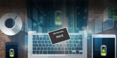
Image sensor minimises distortion in machine vision and mixed reality applications

A combination of a high dynamic range and pixel design means that the AR0234CS CMOS global shutter image sensor by ON Semiconductor delivers image clarity at 120 frames per second.
The 2.3 Mpixel CMOS image sensor, with global shutter technology is designed for a variety of applications including machine vision cameras, augmented reality (AR), virtual reality (VR) and mixed reality (MR) headsets, autonomous mobile robots (AMRs) and barcode readers.

The AR0234CS captures 1080p video and single frames, up to 120 frames per second. It is claimed to have industry-leading shutter efficiency, to produce crisp and clear images by minimising frame-to-frame distortion in high speed scenes and reducing the motion artefacts that other image sensors experience.

The pixel architecture delivers high dynamic range to support lighting conditions from the darkness of night to bright sunlight. The low noise and improved low light response makes it suitable for applications spanning across consumer, commercial and industrial IoT. The extended operating temperature range makes it deployable in challenging outdoor conditions.

As manufacturers automate production, using vision-based systems, the need for quality image sensing is increasing, explains Gianluca Colli, vice president and general manager, Industrial and Consumer Sensor Division (ICSD) Group at ON Semiconductor. As a result, they are demanding optimum size, performance and power in image sensors, he continued.

The sensor also has programmable regions of interest with on-chip histogram, auto exposure control and 5 x 5 statistics engine, fully integrated strobe illumination control, a flexible row and column skip mode, along with horizontal and vertical mirroring, windowing and pixel binning.

Together with the AP1302 image signal processor (ISP), the AR0234CS delivers a comprehensive camera system that can be designed and developed quickly for fast time-to-market, says ON Semiconductor. System designers can access the DevSuite software to evaluate features and capabilities, configure and tune the sensor, and provide a ready-made output that is usable for further image processing.

The AR0234CS is offered in colour and mono variants, with 0 or 28 degree chief ray angle (CRA).

Samples and development hardware are available now through local ON Semiconductor sales support representatives and authorised distributors.

http://www.onsemi.com

> Read More

Neural network accelerator chip enables IoT AI in battery-powered devices

To reduce energy consumption and latency by a factor of over 100 to enable complex embedded inference decisions at the IoT edge, Maxim Integrated has developed the MAX78000 low power neural network accelerated microcontroller.

It moves AI to the edge without performance compromises in battery-powered internet of things (IoT) devices, says the company. It is able to execute AI inferences at less than 1/100th the energy of software solutions to dramatically improve the run-time for battery-powered AI applications. It also enables new, complex AI use cases.

The MAX78000 executes inferences 100x faster than software running on low power microcontrollers and at a fraction of the cost of FPGAs or GPUs, continues Maxim.

Rather than gathering data from sensors, cameras and microphones, sending that data to the cloud to execute an inference, then sending an answer back to the edge, which is challenging due to poor latency and energy performance. Using low power microcontrollers can be used to implement simple neural networks but latency suffers and only simple tasks can be run at the edge. By integrating a dedicated neural network accelerator with a pair of microcontroller cores, the MAX78000 overcomes these limitations, enabling machines to see and hear complex patterns with local, low-power AI processing that executes in real-time.

Applications such as machine vision, audio and facial recognition can be made more efficient as the MAX78000 can execute inferences at less than 1/100th the energy required by a microcontroller. The MAX78000’s specialised hardware is designed to minimise the energy consumption and latency of convolutional neural networks (CNNs). Hardware runs with minimal intervention from any microcontroller core, making operation extremely streamlined. Energy and time are only used for the mathematical operations that implement a CNN. To get data from the external world into the CNN engine efficiently, customers can use one of the two integrated microcontroller cores: the low power Arm Cortex-M4 core, or the even lower power RISC-V core.

The MAX78000EVKIT# includes audio and camera inputs, and out-of-the-box running demos for large vocabulary keyword spotting and facial recognition. Complete documentation helps engineers train networks for the MAX78000 in the tools they are used to using, either TensorFlow or PyTorch.

The MAX78000 is available from authorised distributors. The MAX78000EVKIT# evaluation kit is also available now.

http://www.maximintegrated.com

> Read More

DAC includes non-volatile memory to simplify handheld designs, says Microchip

Microchip claims to have overcome the problems of implementing multi-channel system control or signal outputs using DACs in portable and handheld industrial, communications, consumer or medical systems. To overcome the need for  significant processor overhead for device configuration during power-up, the MCP47/48FxBx8 family of octal 12-bit DACs include non volatile memory and an integrated voltage reference (Vref) source so they can be pre-configured for safe and efficient power-up without relying on the system processor.

“Handhelds and other portable systems are expected to deliver more capabilities in smaller, simpler designs,” said Bryan J. Liddiard, vice president of Microchip’s mixed-signal and linear business unit. “We help achieve this goal with the first DACs that eliminate processor overhead during power-up and provide the channel density, low power consumption and integrated features that today’s compact systems need so they can operate over longer periods using smaller, lighter batteries,” he added.

The inclusion of non-volatile memory means that the MCP47/48FxBx8 DACs can store user-customised configuration data even when powered down. At power-up, all eight channels are then configured to the pre-defined state without burdening the system processor with this overhead.

Integrating a Vref source into the DACs reduces overall system size and complexity while providing the control to meet critical timing for safely driving all power outputs. The devices also have both SPI and I2C serial interfaces for a choice of device communication.

Operating voltage range is 1.8V to 5.5V and the DACs’ low minimum operating voltage and its power efficiency are claimed to improve thermal performance and reliability. The DACs also provide power-on/brown-out reset protection and what is claimed to be one of the industry’s fastest settling times at five micro seconds. They also operate in the extended temperature range (i.e. -40 to +125 degrees C) for industrial and automotive applications.

The MCP47/48FxBx8 family of DACs is available for volume orders. The family includes 8-, 10- and 12-bit resolution devices in a 20-lead VQFN 5.0 x 5.0mm package and a 20-lead TSSOP package.

http://www.microchip.com

> Read More

Renesas says RA6M4 MCU family advances security for IoT

RA6 series microcontrollers (MCUs) from Renesas now include nine new RA6M4 group MCUs. These additions bring the RA family up to 42 MCUs. The latest 32-bit MCUs boost operating performance up to 200MHz using the Arm Cortex-M33 core based on Armv8-M architecture with Arm TrustZone technology.

The RA6M4 MCUs are supported by the Flexible Software Package (FSP) and Renesas’ partner ecosystem of software and hardware building blocks for RA6M4 MCUs and FSP to address industry 4.0, building automation, metering, healthcare, and home appliance applications.

The MCUs have large embedded RAM with parity/ECC, low power consumption, and benefit from the Arm developer and tools ecosystem. According to Renesas, the RA6M4 MCUs speed the development of intelligent IoT edge and endpoint devices. Renesas’ enhanced Secure Crypto Engine incorporates multiple symmetric and asymmetric cryptography accelerators, advanced key management, security lifecycle management, tamper detection, and increased resistance to side-channel attack, in addition to Arm TrustZone technology. These integrated security features enable customers to realise lower bill of materials (BoM) cost and secure element functionality in IoT designs, Renesas says.

“[The RA6M4 MCUs] offer customers best-in-class performance and security enhancements built with Arm Cortex-M33 cores that clearly deliver more memory, memory interface expansion, better power efficiency and wake-up time, and more connectivity options,” said Roger Wendelken, senior vice president of Renesas’ IoT and Infrastructure Business Unit. “

“IoT edge and endpoint technologies are opening up new opportunities for developers to build smaller devices, with greater privacy and less dependence on the cloud,” said Dipti Vachani, senior vice president and general manager, Automotive and IoT Line of Business at Arm. “The RA6M4 MCUs move intelligence closer to the data, with Arm TrustZone technology built in to ensure privacy and data integrity, helping securely accelerate the growth of IoT,” he added.

The RA6M4 MCUs are built on an efficient 40nm process, to drive power consumption down to 99 microA/MHz while running the CoreMark algorithm from flash. The MCUs also support fast wakeup times of 30 micro seconds from standby using an on-chip oscillator. The high integration up to 1Mbyte code flash memory and 256kbyte of SRAM (64kbyte with ECC) also make the RA6M4 MCUs well suited for low power and safety applications.

The RA6M4 with Flexible Software Package (FSP) allows customers to re-use their legacy code and combine it with software from partners across the Arm ecosystem to speed implementation of complex connectivity and security functions. The FSP includes FreeRTOS and middleware, offering a premium device-to-cloud option for developers. These out-of-box options can be easily replaced and expanded with any other RTOS or middleware. It also provides a host of efficiency enhancing tools for developing projects targeting the RA6M4 MCUs. The e2 studio integrated development environment  (IDE) provides a familiar development cockpit from which the key steps of project creation, module selection and configuration, code development, code generation, and debugging are all managed. FSP uses a GUI to simplify the process and dramatically accelerate the development process.

The RA6M4 MCUs are available now from Renesas’ worldwide distributors.

http://www.renesas.com

> Read More

About Smart Cities

This news story is brought to you by smartcitieselectronics.com, the specialist site dedicated to delivering information about what’s new in the Smart City Electronics industry, with daily news updates, new products and industry news. To stay up-to-date, register to receive our weekly newsletters and keep yourself informed on the latest technology news and new products from around the globe. Simply click this link to register here: Smart Cities Registration