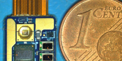
Fusion Design platform enables first-pass silicon for Armv9-based SoCs

Multiple SoC tape-outs at early adopters of the Arm Cortex-X2, Cortex-A710, and Cortex-A510 CPUs based on Arm’s Armv9 architecture, Arm Mali-G710 GPUs and Arm DynamIQ Shared Unit-110, have been announced. They were achieved using Synopsys’ EDA and IP, including Fusion Design Verification Continuum and DesignWare Interface IP.

The latest SoCs, developed for high end consumer devices, use Armv9’s performance and power efficiency enhancements and jointly developed flows and methodologies targeting the latest 5nm, 4nm and 3nm process technologies.

The EDA tools and IP provide designers with the leading, SoC-centric, and power-first software-to-silicon solution, says Synopsys, to hasten the achievement of the maximum performance per Watt across various use cases, including specialised artificial intelligence (AI), digital signal processing (DSP) and virtual and augmented reality (XR) workloads which are expected to be broadly deployed in next generation consumer devices.

“Based on the Armv9 architecture, the Arm Total Compute solution is designed to deliver a step-change in compute performance and efficiency while providing the levels of native security and trust needed in an increasingly data-centric and connected world,” said Paul Williamson, senior vice president and general manager, Client Line of Business, Arm.

Designers creating Armv9-based SoCs for a range of markets, including smartphones, laptops, PCs, digital TVs, wearables, and augmented- and virtual-reality applications, select Synopsys’ portfolio of integrated digital, verification and interface IP solutions to achieve optimum differentiation and the fastest time-to-market, says the company.

“Data is becoming an ever-increasing and important currency in this knowledge-driven world, and its timely, efficient and secure processing is paramount in shaping a safe, information-leveraged future,” said Shankar Krishnamoorthy, general manager of the Digital Design Group at Synopsys. “Our broad portfolio of optimised design, verification, IP, software security and software quality solutions have been aggressively co-optimised with Arm to enable a new wave of high-value applications based on the Armv9 architecture, establishing the new benchmark for trustworthy, power-centric performance.”

According to Synopsys, the Fusion Design Platform delivers unprecedented full-flow quality-of-results and time-to-results. Fusion Technology redefines conventional EDA tool boundaries – test, synthesis, place-and-route, and signoff – by sharing common, best-in-class engines, enabling broad-flow optimisations and wide-ranging margin reduction for performance per Watt and time to results.

Early adopters of Arm’s Armv9 mobile solution are using Synopsys’ Verification Continuum Platform solutions optimised for Arm, including Virtualizer Development Kit (VDK) with Arm Fast Models for Cortex-X2, Cortex-A710, Cortex-A510 CPUs and Mali-G710 GPUs, VCS simulation, Verdi for hardware and software debug, Verification IP for the latest Arm AMBA interconnect, ZeBu Server and HAPS hardware to accelerate hardware-software development and power and performance validation to reduce time-to-market.

The DesignWare Interface IP portfolio provides the performance, power efficiency, security and real-time connectivity for Arm-based systems implementing the latest Cortex CPUs and Mali GPUs. Synopsys’ IP portfolio of controllers and PHYs supporting the latest protocols such as PCI Express, DDR, MIPI and USB, is optimised for the rapid development of Arm-based SoCs.

Synopsys QuickStart Implementation Kits (QiKs) include implementation scripts and reference guides and enable early adopters to accelerate time-to-market and achieve their demanding performance per Watt targets.

http://www.synopsys.com

> Read More

Lattice enhances sensAI stack to simplify AI/ML deployment

Enhancements to the Lattice sensAI solution stack are designed to accelerate artificial intelligence / machine learning (AI/ML) application development on Lattice’s low power FPGAs. The company has added support for the Lattice Propel design environment for embedded processor-based development and the TensorFlow Lite deep-learning framework for on-device inferencing.

Support for the TensorFlow Lite framework reduces power consumption and increases data co-processing performance in AI/ML inferencing applications. TensorFlow Lite runs anywhere from two to 10 times faster on a Lattice FPGA than it does on an Arm Cortex-M4-based microcontroller, reports Lattice.

Another enhancement is the stack’s support for Lattice Propel environment’s GUI and command line tools to create, analyse, compile, and debug both the hardware and software design of an FPGA-based processor system. Even developers unfamiliar with FPGA design can use the tool’s drag and drop interface to create AI/ML applications on low power Lattice FPGAs with support for RISC-V-based co-processing, claims Lattice.

Lattice sensAI Studio is a GUI-based tool for training, validating, and compiling ML models optimised for Lattice FPGAs.

The Lattice sensAI Studio design environment is for end-to-end ML model training, validation, and compilation. Developers can implement sensAI 4.0 using a simple drag and drop interface to build FPGA designs with a RISC-V processor and a convolutional neural network (CNN) acceleration engine to quickly implement ML applications on power-constrained edge devices.

Leveraging advances in ML model compression and pruning, sensAI 4.0 can support image processing at 60 frames per second with QVGA resolution or 30 frames per second with VGA resolution.

Lattice has also responded to the demand in multiple end markets to add support for low power AI/ML inferencing for applications like object detection and classification. AI/ML models can be trained to support applications for a range of devices that require low power operation at the edge, including security and surveillance cameras, industrial robots, and consumer robotics and toys. The sensAI solution stack helps developers rapidly create AI/ML applications that run on flexible, low power Lattice FPGAs, says the company.

http://www.latticesemi.com

> Read More

Nordic introduces first PMIC for tight spaces

Nordic Semiconductor’s first power management device is the nPM1100, a power management integrated circuit (PMIC). It combines a USB compatible Li-ion/Li-Po battery charger and DC/DC buck regulator in a compact WLCSP for space-constrained applications.

The low IQ PMIC for the company’s nRF52/nRF53 series SoCs and other compatible devices. The 400mA battery charger and 150mA DC/DC step down regulator is integrated with a USB-compatible input regulator with overvoltage protection in a WLCSP which measures 2.075 x 2.075mm. The PMIC ensures reliable power supply and stable operation for the nRF52 and nRF53 series multi-protocol SoCs and maximises the application battery life, says Nordic. It can be used as a generic PMIC for any application using rechargeable Lithium Ion or Lithium Polymer batteries.  Its form factor makes it suitable for wearables, connected medical devices, and other space-constrained applications.

The nPM1100’s battery charger can bypass the first regulator stage of Bluetooth Low Energy (BLE) applications based on nRF52 and nRF53 SoCs. In this configuration the buck regulator’s high efficiency reduces overall system power consumption while its 150mA current capability increases the current available for other system components from approximately 10 to 100mA.

The nPM1100 features a low quiescent current (IQ) of 700nA (typicall) which can be further reduced to 470nA in “ship mode” (i.e disabling the power output, removing the need for an external power switch), which minimises battery lifetime impact on products in transit. The power management solution takes up as little as 23mm2 of PCB area, including passive components (rising to 27mm2 when optimised for performance).

The nPM1100 input regulator draws its power from either a 4.1 to 6.6V USB input or from a 2.3 to 4.35V connected battery input. It can supply a 3.0 to 5.5V unregulated voltage to the application at up to 500mA output current. The PMIC supports USB standard downstream port (SDP), charging downstream port (CDP) and dedicated charger port (DCP) detection. The input regulator includes over-voltage protection for transient voltage spikes up to 20V.

The battery charger is JEITA-compliant and will charge the application’s Li-ion/Li-Po battery with a resistor-selectable charge current from 20 to 400mA and a selectable termination voltage of 4.1 or 4.2V. The charger includes battery thermal protection and automatic selection from three charging modes: automatic trickle, constant current and constant voltage. The charger also features a discharge current limitation.

The DC/DC buck voltage regulator runs at more than 90 per cent efficiency down to below 100 microA load current. It takes its power from the input system regulator and provides up to 150mA current at a selectable 1.8, 2.0, 2.7 or 3.0V regulated output voltage. The regulator features soft start up and automatic transition between hysteretic and pulse width modulation (PWM) modes. It also supports a forced PWM mode for clean power operation.

No configuration software is required as all settings are pin configurable. The PMIC is compatible with all devices designed to operate within the output voltages and supply currents the chip can deliver. The product’s operating temperature range is -40 to 85 degrees C.

Nordic also offers the nPM1100 evaluation kit with switches for all selectable settings, buttons to enter and exit ship mode and connectors for batteries, USB and headers for all pins on the PMIC. It can be powered by USB via the on-board micro-USB port, from an external DC power supply through header pins or from battery power via the battery connectors on one of the headers.

http://www.nordicsemi.com

> Read More

LTE CAT-M1 module eliminates gateways in IoT networks

Pre-tested and certified RYZ014A Cat-M1 cellular modules by Renesas are the company’s first cellular IoT modules to support the specification. Devices can directly connect to the internet using an existing communication infrastructure owned by mobile network operators, without the need for a gateway, says Renesas. This makes it economical to connect each device, which is beneficial when installing larger networks that require a low cost per unit.

To build a wireless IoT project from scratch, the RYZ014A module includes RF regulatory certification, PTCRB/GCF (network operators) certification and carrier certification for the customer’s network operator of choice.

The module has been certified with all major radio frequency regulations in the world as well as with leading network operators in North America, APAC and European countries. 

The RYZ014A module is suitable for metering, smart home, infrastructure and industrial markets, where they can seamlessly interface Renesas microcontroller-based applications to the internet through their cellular network, for example Bluetooth Low Energy, Ultra-wide band (UWB) and Wi-SUN protocols.

Renesas has partnered with 4G and 5G chip and IoT module supplier, Sequans Communications, to provide the Monarch LTE CAT-M1 hardware and software technology used in the module.

Renesas offers customers a web-based portal, managed by ONE Tech, that provides easy access to read sensor values and manage SIM card plans remotely, reducing operating cost. ONE Tech’s embedded AI and cloud technology, with the Renesas CAT-M1 module offers embedded intelligence with an enterprise-grade platform, allowing customers to build, manage and scale smart machines in a cost-effective end-to-end ecosystem, says Renesas.

Support for world-wide frequency bands in a single design removes the need to create multiple customer platforms for different global regions, points out Renesas. There is also high output power supporting both power class options 20 and 23dBm and low current consumption in power saving mode of only 1.0 microA

The RYZ014A module and the RYZ014A-EVK evaluation kits are available now.

 The RYZ014A modules can be combined with components from Renesas, such as power ICs, Li-ion battery charger, light-to-digital sensor, and RA family microcontrolelrs to create systems, such as remote industrial process monitoring and automatic plant watering with an LTE Connection.

http://www.reneasas.com

> Read More

About Smart Cities

This news story is brought to you by smartcitieselectronics.com, the specialist site dedicated to delivering information about what’s new in the Smart City Electronics industry, with daily news updates, new products and industry news. To stay up-to-date, register to receive our weekly newsletters and keep yourself informed on the latest technology news and new products from around the globe. Simply click this link to register here: Smart Cities Registration