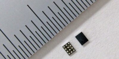
Clock buffers and multiplexers meet PCIe Gen6 specifications

Believed to be the first clock buffers and multiplexers on the market to meet stringent PCIe Gen6 specifications, the RC190xx clock buffers and RC192xx multiplexers have been released by Renesas. 

The release comprises 11 clock buffers and four multiplexers. The devices, which also support and provide extra margin for PCIe Gen5 implementations, complement Renesas’ low-jitter 9SQ440, 9FGV1002 and 9FGV1006 clock generators for PCIe Gen6 timing for data centre / cloud computing, networking and high-speed industrial applications.

The PCIe Gen6 standard supports extremely high data rates of 64Gtransfers per second while requiring very low clock jitter performance of less than 100fs RMS. The RC190xx clock buffers and RC192xx multiplexers have PCIe Gen6 additive jitter specs of only 4fs RMS, making them virtually noiseless, says Renesas. The company claims this means they future-proof designs for the next generation of industry standards.

“PCIe Gen6 timing will be at the heart of new equipment in data centers, high-speed networking and other applications,” said Zaher Baidas, vice president of the Timing Products division at Renesas. 

“It will be interesting to see the innovative implementations that result from this new capability, especially when considering how solutions for the emerging Chiplet market are starting to evolve, with the need for increasing speed and bandwidth as an underlying constant,” comments Rich Wawrzyniak, principal analyst for Semico Research.

The PCIe Gen6 clock buffers and multiplexers offer 1.4ns in-out delay, 35ps out-out skew and -80dB PSRR (power supply rejection ratio) at 100kHz in addition to low 4fs PCIe Gen6 additive jitter. 

Selectable SMBus addresses facilitate the use of multiple devices while SMBus write-protect feature enhances system security. 

The devices represent 30 per cent space-saving compared to earlier devices, adds Renesas.

Other features are loss-of-signal (LOS) output supports system monitoring and redundancy, a four-wire side-band interface to support high speed serial output enable / disable and device daisy-chaining. In addition, power down tolerant (PDT) and flexible start-up sequencing (FSS) features ensure good behaviour under abnormal system conditions, the company claims.

The RC190xx buffers are offered in 4-, 8-, 13-, 16-, 20- and 24-output configurations. The RC192xx multiplexers include 2-, 4-, 8- and 16-output versions. They are offered in packages as small as 3.0 x 3.0mm. 

All of the new devices are available now, and Renesas also offers an evaluation board schematic. 

http://www.renesas.com

> Read More

Virtual development environment for accelerates automotive development

A virtual development environment announced by Renesas Electronics enables  development and operational evaluation of automotive application software to support the latest requirements of electrical/electronic architecture (E/E architecture). 

The environment includes a virtual turnkey platform, which allows engineers to develop application software before devices or evaluation boards are available. There is also a multi-core debug and trace tool, which enables users to analyse and evaluate software as if running on an actual chip. 

“With the evolution of E/E architecture, there is an increasing demand for software design that can maximise performance at a system level,” explains Hiroshi Kawaguchi, vice president, Automotive Software Development division at Renesas. At the same time, the increasing time and cost associated with software development have become a big challenge. “Our integrated software development environment that can be used across gateway systems, ADAS, and xEV development, enables customers to benefit from the scalability of Renesas products such as R-Car and the RH850 family for both software and hardware development.”

 The virtual turnkey platform application software development environment consists of the R-Car Virtual Platform (R-Car VPF) development environment and a software development kit (R-Car SDK) that includes pre-tested software libraries and sample code. R-Car VPF is based on Virtualizer Development Kits (VDKs) from Synopsys, and integrates virtual models of IP specific to R-Car to customise for R-Car devices. By overlaying the R-Car SDK engineers can immediately start development of application software virtually. The platform accurately recreates the behaviour of the chip and eliminates the need to build up a development environment with a physical evaluation board. Multiple users can also develop software simultaneously on separate PCs or servers.

The next step is to integrate the software and verify that it runs on a single chip. Software components share resources such as the multiple CPUs and IPs on R-Car SoCs. If operational problems are detected after the software components are integrated, it requires a tremendous amount of work to analyse and solve them, explains Renesas. The Multicore Debug and Trace tool analyses and identifies the causes of errors occurring from the interaction of the multiple hardware resources in R-Car SoCs. This enables synchronous and simultaneous debugging of the entire heterogeneous architecture of R-Car without using the actual device.

The development environment is available for the R-Car S4 SoC for automotive gateways. Renesas has plans to support the R-Car V4H as well as future versions of R-Car products and RH850 automotive MCUs.

https://www.renesas.com

> Read More

mmW 5G chipset addresses 5G NR FR2 spectrum 

Designers can reduce the complexity of 5G radio and reduce the number of components required, using a millimeter wave (mmW) 5G front-end chipset by Analog Devices. 

It comprises two single channel (1T1R) up / down converters (UDCs) and two dual polarisation 16-channel beamformer devices on a CMOS process. The power efficiency and linear output power provided by the beamformers enable size, weight, power, and cost reduction in mmW phased array designs compared to competing solutions, claims Analog Devices. The full-band UDCs with high drive level eliminate the need for frequency band variants and absorb driver stages for bill of materials savings. 

The mmW 5G front-end chipset includes four devices from Analog Devices, the ADMV4828, the ADMV4928, the ADMV1128 and ADMV1139. 

The ADMV4828 is a16-channel beamformer covering the 24 to 29.5GHz band in a single IC with more than 12.5dBm output power at three per cent error vector measurement (EVM) with a 400MHz 64QAM 5G NR (new radio) waveform while consuming only 310mW per channel.

The ADMV4928 is a 16-channel beamformer covering the 37 to 43.5GHz band in a single IC with above 11.5dBm output power at three per cent EVM with a 400MHz 64QAM 5G NR waveform while consuming only 340mW per channel.

The ADMV1128 is the company’s 24GHz to 29.5GHz wideband UDC with optional on-chip RF switch and hybrid, x2 /x4 local oscillator (LO) multiplier modes and baseband IQ support.

The fourth element is the ADMV1139, a 37 to 50GHz wideband UDC suitable for the upcoming 47GHz, as well as the 37 to 43.5GHz 5G NR bands. The single IC has optional on-chip RF switch and hybrid, with baseband IQ support.

The chipset enables seamless operation of phased array calibration functions online in the field in addition to factory non-volatile memory (NVM) through patented IP. This allows OEMs to move beyond the constraints of legacy NVM-only designs limited to one-time factory calibration of the beamformer, which does not address non-idealities external to the ICs and results in sub-optimal calibration results.

Analog Devices adds that mmW 5G deployment highlights the need for operators to expand their network footprint with more energy efficient, lightweight, and reliable radios. This requires highly linear, compact, and power efficient wideband products that allow design reuse over multiple bands without compromising on quality and performance. Analog Devices says that this mmW 5G front-end chipset allows OEMs to depart from the narrowband paradigm where competing solutions have traded-off design execution difficulty and RF performance for bandwidth, while also outsourcing critical pieces of IP such as packaging, test, and thermal modelling. 

The company also offers in-house quality management and package development, enabling engineers to create reliable, fully optimised, and customisable 5G radios quickly. 

http://www.analog.com

> Read More

NXP drives forward with radar sensor SDK

Radar signal processing algorithms in NXP’s Premium Radar software development kit (SDK) enable developers to enhance radar system performance. It leverages tight coupling of NXP’s software algorithms with its S32R4x radar processor family for improved safety and differentiation. The proprietary radar algorithm library allows quick integration of proven algorithms into radar sensor applications, helping to speed radar sensor development and reduce R&D investment, said NXP. 

The initial release, expected to be available for evaluation during 2022, includes three algorithm packages for interference mitigation, MIMO waveform optimisation and angular resolution enhancement.

Radar is increasingly used in vehicle applications like automated emergency braking and adaptive cruise control. In addition, legislation and regulations mandate more demanding features for blind-spot detection, turn assistant, front and rear cross-traffic and people detection, requiring more radar nodes per vehicle. Another contributor is the consumer demand for a safer and more comfortable driving experience which is accelerating the transition to L2+, offering comfort features close to L3 autonomous driving, said NXP. 

In about five years, cars will carry twice as many radar sensors as today, and over 90 per cent of the radar sensors will be emitting in the same 77 to 79GHz band. 

“We expect the triple acceleration of automotive radar to continue over the next decade, with more cars equipped with radar sensors, an increasing number of sensor nodes per car and more performant sensors being deployed,” said Huanyu Gu, director product marketing and business development ADAS, NXP. For vehicle OEMs and Tier 1 suppliers, this “poses a need for interference mitigation, MIMO waveform optimisation and augmented sensor resolution,” he explained. NXP’s Premium Radar SDK’s advanced algorithms aim to address all these challenges, enabling customers to optimally leverage the S32R4x radar processor hardware, he added.

Optimised MIMO waveforms enable radar sensors with higher resolution and longer reach in modulation schemes which allow more transmitters to operate simultaneously. They code the individual transmit antenna signals to ensure they can be differentiated on the receiver side. Higher resolution sensors are used for both corner and front radar applications to support more accurate object separation and classification for use cases such as vulnerable road user detection or park assist functions. 

The Premium Radar SDK implementation complies with International Automotive Quality Management standards IATF 16949:2016 and ASPICE Level 3 requirements. 

NXP offers OEM and Tier 1 suppliers two evaluation options under an evaluation license agreement. The MATLAB-based version delivers the algorithms as compiled code to allow developers to understand what the SDK does by feeding customer test vectors, computing and visualising the output vectors. Providing bit accuracy, the microcontroller-based evaluation option includes the algorithm binary files to run on the NXP target radar processor evaluation board and demonstrates the real time performance of the SDK.

http://www.nxp.com

> Read More

About Smart Cities

This news story is brought to you by smartcitieselectronics.com, the specialist site dedicated to delivering information about what’s new in the Smart City Electronics industry, with daily news updates, new products and industry news. To stay up-to-date, register to receive our weekly newsletters and keep yourself informed on the latest technology news and new products from around the globe. Simply click this link to register here: Smart Cities Registration