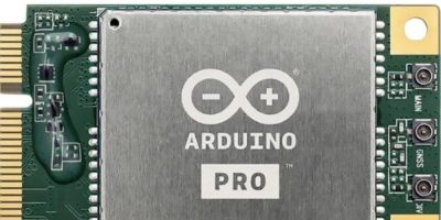
Renesas announces ultra-fast MRAM test chip for IoT and AI devices

Renesas has announced that it has developed circuit technologies for an embedded spin-transfer torque magnetoresistive random-access memory (STT-MRAM, hereinafter MRAM) test chip with fast read and write operations. Fabricated using a 22-nm process, the microcontroller unit (MCU) test chip includes a 10.8-megabit (Mbit) embedded MRAM memory cell array. It achieves a random read access frequency of over 200 MHz and a write throughput of 10.4-megabytes-per-second (MB/s).

As IoT and AI technologies continue to advance, MCUs used in endpoint devices are expected to deliver higher performance than ever. The CPU clock frequencies of high performance MCUs are in the hundreds of MHz, so to achieve greater performance, read speeds of embedded non-volatile memory need to be increased to minimise the gap between them and CPU clock frequencies. MRAM has a smaller read margin than the flash memory used in conventional MCUs, making high speed read operation more difficult. On the other hand, for write performance, MRAM is faster than flash memory because it requires no erase operation before performing write operations. However, shortening write times is desirable not only for everyday use, but also for cost reduction of writing test patterns in test processes and writing control codes by end product manufacturers.

MRAM reading is generally performed by a differential amplifier (sense amplifier) to determine which of the memory cell current or the reference current is larger. However, because the difference in memory cell currents between the 0 and 1 states (the read window) is smaller for MRAM than for flash memory, the reference current must be precisely positioned in the centre of the read window for faster reading. The newly developed technology introduces two mechanisms. The first mechanism aligns the reference current in the centre of the window according to the actual current distribution of the memory cells for each chip measured during the test process. The other mechanism reduces the offset of the sense amplifier. With these adjustments, faster read speed is achieved.

Furthermore, in conventional configurations, there is large parasitic capacitance in the circuits used to control the voltage of the bitline so it does not rise too high during read operations. This slows the reading process, so a Cascode connection scheme is introduced in this circuit to reduce parasitic capacitance and speed up reading.

Thanks to these advances, Renesas can achieve the world’s fastest random read access time of 4.2 ns. Even taking into consideration the setup time of the interface circuit that receives the MRAM output data, we can realize the random read operation at frequencies in excess of 200 MHz.

For the write operation, the high-speed write technologies for embedded STT-MRAM announced in December 2021 improved write throughput by first applying write voltage simultaneously to all bits in a write unit using a relatively low write voltage generated from the external voltage (IO power) of the MCU chip through a step-down circuit, and then used a higher write voltage only for the remaining few bits that could not be written. This time, Renesas takes into account that because the power supply conditions used in test processes and by end product manufacturers are stable, the lower voltage limit of the external voltage can be relaxed. Thus, by setting the higher step-down voltage from the external voltage to be applied to all bits in the first phase, write throughput can be improved 1.8-fold.

Combining the above new technologies, a prototype MCU test chip with a 10.8Mbit MRAM memory cell array was fabricated using a 22 nm embedded MRAM process. Evaluation of the prototype chip confirmed that it achieved a random read access frequency of over 200 MHz and a write throughput of 10.4 MB/s at a maximum junction temperature of 125°C.

The test chip also contains 0.3 Mbit of OTP (Note 2) that uses MRAM memory cell breakdown to prevent falsification of data. This memory can be used to store security information. Writing to OTP requires a higher voltage than writing to MRAM, making it more difficult to perform writing in the field, where power supply voltages are often less stable. However, by suppressing parasitic resistance within the memory cell array, this new technology also makes writing in the field possible.

https://www.renesas.com

> Read More

Kontron announces KISS Rackmount PC in 1U format with high performance and energy efficiency

Kontron has announced the KISS 1U V4 ADL Rackmount PC, a compact member of the KISS product family for demanding industrial applications. The robust and space-saving 1U industrial computer scores with a motherboard developed and manufactured in Germany based on 12th/13th generation Intel Core processors and thus with more performance, increased reliability and better energy efficiency. This makes it particularly suitable for use in demanding industrial environments, as well as for high-end image processing and SCADA/MES applications, but also in person-related areas such as control technology and medical environments.

The powerful systems of the KISS V4 ADL series are based on Kontron motherboards with Intel Core i9/i7/i5/i3 processors of the 12th/13th generation with up to 24 cores. Two GbE ports, one with up to 2.5 Gb/s and eight external USB ports including USB-C ensure high data throughput and connectivity. Two DIMM sockets, each with up to 64 GB, provide sufficient RAM. Equipped with DDR5 UDIMM memory, a significant increase in performance is also achieved. A wide range of internal and hot-swappable external storage media enables customized systems for any application.

A particularly compact and powerful system is now available for the industrial automation, video surveillance and medical technology markets in particular, which opens up a new dimension in graphics applications with its four DisplayPort interfaces. Powerful power supply units are also available for AI and machine learning applications, allowing the installation of high-end GPU cards.

Like all members of the new KISS family, the KISS 1U V4 ADL also supports the highest security standards and allows real-time applications for control tasks in the control cabinet or data consolidation in the local cloud thanks to TSN features.

The entire KISS product family meets high requirements in extreme environments: Thanks to the effective cooling concept, the rackmount system can withstand ambient temperatures from 0 °C to +50 °C during 24/7 continuous operation. The high shock and vibration resistance also predestines the KISS V4 ADL series for robust industrial applications.

Customer-specific adaptations, such as individual front covers, can be implemented quickly and cost-effectively thanks to the modular concept, even for small and medium quantities.

https://www.kontron.com/en/products/kiss-1u-v4-adl/p183444

> Read More

Cadence unveils Millennium Platform the industry’s first accelerated digital twin  

Cadence has announced the Cadence Millennium Enterprise Multi-physics Platform, the industry’s first hardware/software (HW/SW) accelerated digital twin solution for multiphysics system design and analysis. Targeted at one of the biggest opportunities for greater performance and efficiency, the first-generation Cadence Millennium M1 accelerates high-fidelity computational fluid dynamics (CFD) simulations. Available in the cloud or on premises, this turnkey solution includes graphics processing units (GPUs) from leading providers, extremely fast interconnections and an enhanced Cadence high-fidelity CFD software stack optimised for GPU acceleration and generative AI. Millennium M1 instances can be fused into a unified cluster, enabling customers to achieve an unprecedented same-day turnaround time and near-linear scalability when simulating complex mechanical systems.

Designing mechanical systems for new levels of performance and efficiency has become a key priority in the automotive, aerospace and defence (A&D), energy and turbo-machinery industries. To optimise performance and reduce greenhouse gases, automotive designers are focused on improving fuel efficiency, reducing drag and noise, and extending electric vehicle range. Increasing efficiency, reducing carbon emissions and reducing maintenance frequency are top of mind for A&D and turbo-machinery design engineers. Advances in multi-physics simulation technology are critical to achieving these goals. Performance, accuracy, capacity and accelerated computing are all essential to enabling digital twin simulations that explore more design innovations, providing confidence that they will function as intended before undertaking prototype development and testing.

The Millennium Platform addresses these needs. Highlights and benefits include:
* Performance: Combines best-in-class GPU-resident CFD solvers with dedicated GPU hardware to provide supercomputer-equivalent throughput per GPU of up to 1000 CPU cores
* Efficiency: Reduces turnaround time from weeks to hours with 20X better energy efficiency compared to its CPU equivalent
* Accuracy: Leverages Cadence Fidelity CFD solvers to provide unmatched accuracy to address complex simulation challenges
* High-Performance Computing: Built with an extensible architecture and massively scalable Fidelity solvers to provide near-linear scalability on multiple GPU nodes
* AI Digital Twin: Rapid generation of high-quality multi-physics data enables generative AI to create fast and reliable digital twin visualisations of the optimal system design solution
* Turnkey Solution: The industry’s first solution that couples GPU compute with modern and scalable CFD solvers, providing an optimised environment for accelerated CFD and multidisciplinary design and optimisation
* Flexibility: Available with GPUs from leading vendors, in the cloud with minimum 8 GPU configurations, or on premises with a minimum 32 GPU configuration—providing a flexible and scalable solution to fit each customer’s deployment needs

“Throughout our 35-year history, Cadence has been focused on increasing performance with no loss of accuracy for the most challenging computational applications. Algorithmic throughput remains a key priority, and we’re now leveraging generative AI to harvest knowledge gained from massive quantities of design and simulation data,” said Ben Gu, corporate vice president of R&D for multi-physics systems analysis at Cadence. “Our revolutionary Millennium platform is a giant leap forward, delivering unprecedented acceleration and scalability of digital twin and AI applications. CFD is poised to benefit greatly from performance and efficiency gains, and the tremendous power of the Millennium M1 is disrupting industries that must explore more design innovations and bring them to market faster.”

https://www.cadence.com

> Read More

NeoMesh click boards speed development of ultra-low power, massively scalable IoT and Cloud-based sensor networks

Mikro Elektronika today announced three new NeoMesh Click boards that are ideal for wireless mesh networking. The Click boards eliminate the need for engineers to create any development PCB hardware themselves, enabling them to initiate Proof-of-Concept testing of the NeoMesh network protocol stack in a real application quickly and at minimal cost.

The Click Boards feature NeoCortec’s compact, low-power NC1000 and NC2400 network modules which address a broad range of applications based on IoT and Cloud-based sensor networks, including smart building and smart workplace, metering, security, agriculture, transportation, industry 4.0, medical and food distribution. Three versions of NeoMesh Click are available, one for each of the communication modules which operate at 868MHz, 915MHz and 2.4 GHz. Average power consumption is as low as 20uA.

Explains Thomas Steen Halkier, CEO of NeoCortec: “The NeoMesh protocol is a natural choice when building battery-powered, highly scalable and reliable wireless sensor networks. Now, developers have access to a large selection of MCU, sensor and other boards which can simply ‘Click’ together to form a prototype device.”

Click boards follow mikroBUS a modular prototyping add-on board standard invented by MIKROE, enabling design engineers to change peripherals easily, cutting months off development time. Any Click board can be connected to the microcontroller or microprocessor on a main board. Many leading microcontroller companies including Microchip, NXP, Infineon, Dialog, STM, Analog Devices, Renesas and Toshiba now include the mikroBUS socket on their development boards.

https://www.neocortec.com


> Read More

About Smart Cities

This news story is brought to you by smartcitieselectronics.com, the specialist site dedicated to delivering information about what’s new in the Smart City Electronics industry, with daily news updates, new products and industry news. To stay up-to-date, register to receive our weekly newsletters and keep yourself informed on the latest technology news and new products from around the globe. Simply click this link to register here: Smart Cities Registration