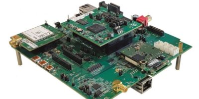
CommAgility supports scalable 5G network tester for Viavi

The TM500 is a scalable test system for validating the performance of cellular networks, including 3GPP 4G, 4.5G, and 5G. CommAgility is supporting Viavi Solution in the 5G TM500 network tester. The system tests network performance as experienced by end users, across multiple cells and different radio access technologies.

Virtually all 4G and 5G base stations have been validated using the Viavi TM500, said Evan Gray, vice president product management at Viavi. CommAgility has supported TM500 with the development of 4G solutions since 2007.

He continued that the latest module has enabled the company to streamline the development process to upgrade the TM500 to 5G.

“We’re delighted to extend our long relationship with Viavi by providing signal processing cards for their 5G base station test systems,” said Edward Young, vice president and general manager at CommAgility. “By incorporating our standards-based processing boards they have been able to streamline development, and to focus efforts on customer requirements,” he added.

CommAgility’s hardware provides signal processing and flexible I/O options enabling OEMs to bring 5G products to market quickly. Baseband processing and RF cards include Texas Instruments SoCs from four to 16 DSP cores and Xilinx high-density Virtex-7 and Kintex-7 FPGAs, in a variety of form factors including AMC and VPX. The modules also provide fast, flexible I/O including Gen2 RapidIO, Gigabit Ethernet and PCI Express.

Viavi provides network test and monitoring equipment to communications service providers, enterprises, network equipment manufacturers, civil, government, military and avionics customers, supported by a worldwide channel community including Viavi Velocity Partners.

CommAgility designs and manufactures RF and microwave components, modules, systems and instruments for the wireless, telecommunication, satellite, military, aerospace, semiconductor and medical industries.

http://www.commagility.com

> Read More

Advantech launches SMARC module for industrial automation

The first Smart Mobility Architecture (SMARC) module from Advantech is the SOM-2569. The SMARC small form factor computer module targets applications that require low power consumption and upgrades to computing performance. It is bundled with the WISE-PaaS/DeviceOn software to help customers with operations management and ease of maintenance, says Advantech.

The SOM-2569 SMARC module features Intel Atom E3900, Pentium and Celeron N series processors. It measures 82 x 50mm and supports up to three displays simultaneously. It also supports SATA, USB3.0/2.0, COM port, SMBus, and I2C I/O.

There are two LAN controllers that support two RJ45 ports and an on-board wi-fi module and Trusted Platform Module (TPM) and secure boot for enhanced security.

The SOM-2569 is suitable for automation applications, says Advantech, with integrated wi-fi and Bluetooth on-board, and dual 1000base-T interfaces to meet both wireless and cable connectivity requirements. For example, when the wireless LAN connects to an outside network and the wired LAN can connect to two different local area networks simultaneously.

The TPM2.0 and UEFI secure boot protects against cyber intrusions. The UEFI security boot offers a process to ensure that a computer boots up using only software that is trusted by the manufacturer. When the computer starts, firmware checks the signature of each piece of boot software, including firmware drivers and the operating system. If the signatures are good, the PC boots and the firmware gives control to the operating system.

The SOM-2569 complies with IEEE 802.11 a/b/g/n/ac PCIe wi-fi and Bluetooth 4.2 and RF certification.

Advantech’s design and testing processes allows it to offer wireless signal integrity and compatibility and also saves time for system integration. Tests include vibration at 0.028G²/ Hz, 3.5 Grms, bumping at one corner, three edges, six faces and thermal shock resistance, ranging from -40 to +85 degrees C at slope 10 degrees C per minute. Advantech rigorous validation proves SOM-2569 is suitable for use in a harsh environment.

http://www.advantech.com

> Read More

Automotive-grade MOSFETs lead way for small ADAS cameras

The new RV4xxx series enables greater miniaturisation in automotive devices such as ADAS camera modules, says Rohm Semiconductor.

The compact 1.6 x 1.6mm MOSFETs are AEC-Q101-qualified. The MOSFETs are claimed to be the first in the industry to ensure the electrode height on the side of the package (130 micron) required for vehicle applications by using original wettable flank formation technology. The result is a consistent solder quality, says Rohm – even for bottom electrode type products – enabling automatic inspection machines to easily verify solder conditions after mounting. Automotive optical inspection is performed during the assembly process, but the height of bottom electrode components solder cannot be verified after mounting. The RV4xxx series uses a proprietary wettable flank technology that guarantees an electrode height on the side of the package of 130 micron. This is achieved by making a cut into the lead frame on the side of the package before plating. However, burrs resulting from cutting into the lead frame can occur more frequently as the height of the cut increases. Rohm’s method introduces a barrier layer on the entire surface of the lead frame to minimise the occurrence of burrs. This not only prevents component rise and solder defects during mounting, but is the first on the market to ensure a 130 micron electrode height on the side of DFN1616 (1.6 x 1.6mm) packages.

Schottky barrier diodes (SBDs) are commonly used in the reverse connection protection circuits of ADAS camera modules, but the larger currents required by high resolution cameras in advanced vehicle systems, call for the use of compact MOSFETs instead that provide low on resistance and less heat generation.

For example, at a current and power consumption of 2.0A and 0.6W, respectively, conventional automotive MOSFETs can reduce mounting area by 30 per cent compared with SBDs, says Rohm. In addition, adopting bottom electrode MOSFETs for their heat dissipation characteristics, while still supporting large currents in an even smaller form factor makes it possible to decrease mounting area by as much as 78 per cent compared with conventional SBDs and by as much as 68 per cent compared with conventional MOSFETs.

Samples are available now, with OEM qualities expected in September 2019.

http://www.rohm.com/eu

> Read More

Trio of photocouplers drive industrial applications with lower power budgets

Three 15Mbits per second photocouplers from Renesas Electronics are designed to withstand the harsh operating environments of industrial and factory automation equipment. They have been developed in response to the trend for higher voltage, compact systems for safety standards and eco-friendly designs that require smaller ICs with lower power consumption. The RV1S9x60A family is claimed to have best-in-class low threshold input current (IFHL) ratings. The RV1S9160A (SO5) operates at 2.0mA, the RV1S9060A (LSO5) operates at 2.2mA and the RV1S9960A (LSDIP8) operates at 3.8mA.

Lower power consumption allows the RV1S9x60A photocouplers to suppress power supply heat generation. Operation at high temperatures, up to 125 degrees C (+110 degrees C for RV1S9960A) saves board space by allowing the photocoupler to be mounted near an IGBT or MOSFET power device. The devices are targeted at DC to AC power inverters, AC servo motors, programmable logic controllers (PLCs), robotic arms, solar and wind input power conditioners, and battery management systems for energy storage and charging.

The RV1S9x60A photocouplers feature high common mode rejection (noise tolerance) up to 50 kV/ micro seconds (minimum) to protect microcontrollers and other I/O logic circuits from high voltage spikes while transferring high-speed signals. The RV1S9x60A family also offers a variety of packages with the smallest footprint for each reinforced isolation (up to 690Vrms), and minimum creepage distances of 4.2 to 14.5mm to ensure safe operation.

The RV1S9160A, RV1S9060A and RV1S9960A photocouplers operate at low voltages, from 2.7 to 5.5V. Isolation voltages are 3,750Vrms (RV1S9160A), 5,000Vrms (RV1S9060A), and 7,500Vrms (RV1S9960A).

High temperature operation from -40°C to +125°C (RV1S9160A and RV1S9060A), and from -40°C to +110°C (RV1S9960A)

The supply current is 2.0mA (max), with a low pulse width distortion at 20 nanoseconds (max). Propagation delay is 60 nanoseconds max and propagation delay skew is 25 nanoseconds max.

The RV1S9x60A 15Mbits per second photocouplers are available now from Renesas Electronics’ worldwide distributors.

Renesas Electronics specialises in microcontrollers, analogue, power and SoC products for a range of automotive, industrial, home electronics, office automation, and information communication technology applications.

http://www.renesas.com

> Read More

About Smart Cities

This news story is brought to you by smartcitieselectronics.com, the specialist site dedicated to delivering information about what’s new in the Smart City Electronics industry, with daily news updates, new products and industry news. To stay up-to-date, register to receive our weekly newsletters and keep yourself informed on the latest technology news and new products from around the globe. Simply click this link to register here: Smart Cities Registration