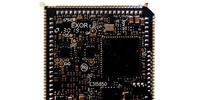
Infineon and Qualcomm enable standard solution for 3D authentication

A reference design developed by Infineon Technologies, working with Qualcomm Technologies is for 3D authentication based on the Qualcomm Snapdragon 865 mobile platform.

The reference design uses the REAL3 3D time of flight (ToF) sensor and enables a standardised integration for smartphone manufacturers.

At CES 2020, Infineon introduced the 4.4 x 5.1mm ToF sensor, describing it as the world’s smallest yet most powerful 3D image sensor with VGA resolution. It can be used for face authentication, enhanced photo features and authentic augmented

Andreas Urschitz, division president power management and multimarket at Infineon, commented: “3D sensors enable new uses and additional applications such as secured authentication or payment by facial recognition. We continue to focus on this market and have clear growth targets”.

Infineon develops the 3D ToF sensor technology in co-operation with the software and 3D time-of-flight system specialist pmdtechnologies.

From this month, Infineon’s REAL3 ToF sensor will enable the video bokeh function for the first time in a 5G-capable smartphone for optimal image effects even in moving images. Using the precise 3D point cloud algorithm and software, the received 3D image data is processed for the application. The 3D image sensor captures 940nm infrared light reflected from the user and the scanned objects. It also uses high-level data processing to achieve accurate depth measurements. The patented SBI (Suppression of Background Illumination) technology offers a wide dynamic measuring range from bright sunlight to dimly lit rooms for robust operation without loss of data processing quality.

pmdtechnologies is a fabless IC company headquartered in Siegen, Dresden and Ulm with subsidiaries in the USA, China and Korea. It claims to be the leading 3D ToF CMOS-based digital imaging technology supplier. Founded in 2002, the company owns over 350 worldwide patents concerning pmd-based applications, the pmd measurement principle and its realisation. The company operates in industrial applications.

http://www.infineon.com

> Read More

Three-phase SiC MOSFET IPM focuses on e-mobility

For e-mobility applications, a three-phase SiC MOSFET intelligent power module (IPM) from Cissoid has been designed to improve time to market for electric vehicle (EV) OEMs.

The IPM technology includes a three-phase water-cooled SiC MOSFET module with built-in gate drivers. For OEMs and electric motor manufacturers willing to adopt SiC-based inverters for more efficient and compact motor drives, the IPM is claimed to optimise the electrical, mechanical and thermal design of the power module and its proximity control for automotive and industrial markets.

The first product in this scalable platform, a three-phase 1200V/450A SiC MOSFET IPM, features low conduction losses, with 3.25mOhms on resistance and low switching losses, with 8.3mJ turn-on and 11.2mJ turn-off energies at 600V/300A. It reduces losses by at least a factor three, says Cissoid, compared with the highest performing IGBT power modules. Cissoid’s module is water-cooled through a lightweight AlSiC pin-fin baseplate for a junction-to-fluid thermal resistance of 0.15°C/W. The power module is rated for junction temperature up to +175 degrees C. The IPM withstands isolation voltages up to 3,600V (50Hz,  60 seconds).

 The built-in gate driver includes three on-board isolated power supplies (one per phase) delivering each up to 5W allowing it to easily drive the power module up to 25KHz and at ambient temperatures up to +125 degrees C. Peak gate current up to 10A and immunity to high dV/dt (>50KV/µs) enable fast switching of the power module and low switching losses. Protection functions include under-voltage lockout (UVLO), active Miller clamping (AMC), desaturation detection and soft shutdown (SSD).

Dave Hutton, CEO at Cissoid, believes: “With this new SiC intelligent power modules, which is the outcome of years of experience in the development of power modules and gate drivers for extreme temperature and voltage environments, we are happy to deliver our first IPM samples to early SiC adopters and to support the automotive industry in its transition towards highly efficient e-mobility solutions.”

http://www.cissoid.com

> Read More

Flat connectors withstand higher operating temperatures

Flat flexible cable/flat printed circuit (FFC/FPC) connectors from Hirose Electric can withstand higher operating temperatures than standard FFC/FPC connectors. The FH67 series withstand temperatures ranging from -55 to +125 degrees C. This heat resistance capability enables the connector to be used in harsh automotive environments.

The FH67 0.5mm pitch connectors are characterised by a single action lock and a vertical connection design. 

The robust FFC/FPC connectors’ one-action lock allows an FFC/FPC to be inserted into the connector without opening the actuator. This can be done with one hand or by automated machinery, says Hirose, saving valuable assembly time and reducing the rates of mating failure. Removing the connector is also easy and can be done by one hand or by robot.

The FH67 series is reliable with an independent two-point spring contact design, which includes a wiping element that reduces contact failure due to dust intrusion.

The ground contacts allow a shielded FFC to be used which prevents EMI. The FH67 series has a height of just 5.2mm, making it suitable for space-constrained design for use in automotive equipment, smart home devices, medical equipment and other portable devices.

Hirose Electric is a Japanese manufacturer of high-quality connectors. It was established in 1937 and uses advanced engineering services, customer service and worldwide manufacturing capabilities to provide technically advanced connector products for many industries including industrial, automotive, consumer, testing, broadcasting, and telecommunications.

Hirose established European offices over 30 years ago to compete internationally in Europe. In 2010, the European offices were merged together to form Hirose Electric Europe. The European headquarters is based in Amsterdam, The Netherlands. Other European branches are located in Germany, UK, France and Italy.

http://www.hirose.com/eu

> Read More

Lattice supports embedded vision with solutions stack

To accelerate low power, embedded vision development such as image sensor bridging, aggregation, splitting and processing, Lattice Semiconductor has introduced the mVision solutions stack with support for the Nexus platform and CrossLink-NX FPGAs.

It includes the modular hardware development boards, design software, embedded vision IP portfolio, reference designs and demos needed to implement sensor bridging, sensor aggregation, and image processing applications found in machine vision, advanced driver assistance systems (ADAS), drones and augmented reality / virtual reality (AR/VR) for the industrial, automotive, consumer, smart home and medical markets.

Initially used in manufacturing, today embedded vision is used in automated assembly and inventory, explained Jeff Bier, founder of the Edge AI and Vision Alliance. “Many of these applications demand small, low cost, low power solutions,” he continued, adding “Solutions stacks, such as sensAI and mVision . . . help developers more easily integrate smart vision capabilities into their product designs.”

Key features of the Lattice mVision solutions stack are the Video Interface Platform (VIP) modular hardware development boards with support for a variety of video and I/O interfaces commonly used in embedded vision applications (including MIPI, LVDS, DisplayPort, HDMI, USB, and others). The VIP development boards currently support Lattice FPGAs including CrossLink, ECP5 and CrossLink-NX, based on the Lattice Nexus platform.

There is also a comprehensive IP Library. The Lattice mVision solutions stack includes ready-to-implement IP cores for interfacing to MIPI and LVDS image sensors, image signal processing pipelines, common connectivity standards like USB and Gigabit Ethernet, and display standards such as HDMI, DisplayPort, and GigE Vision.

The stack supports both of Lattice’s FPGA design tools, Lattice Diamond and Lattice Radiant. The tools automate many common design tasks.

There are also complete reference designs for common embedded vision applications including sensor bridging, sensor aggregation and image processing.

Customers can also access a  network of design service partners, developed by Lattice, for support ranging from developing individual functional design blocks to complete turn-key solutions.

http://www.latticesemi.com/mvision

> Read More

About Smart Cities

This news story is brought to you by smartcitieselectronics.com, the specialist site dedicated to delivering information about what’s new in the Smart City Electronics industry, with daily news updates, new products and industry news. To stay up-to-date, register to receive our weekly newsletters and keep yourself informed on the latest technology news and new products from around the globe. Simply click this link to register here: Smart Cities Registration