InnoPhase IoT, a fabless semiconductor company specialising in low-power Wi-Fi IoT solutions, Eoxys, an IoT solution provider, and Nuvoton, a microcontroller unit (MCU) supplier, are targeting intelligent and secure IoT devices for smart home, industrial and medical automation applications.
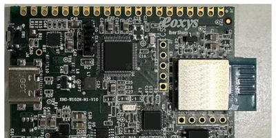
The Eoxys’ Xeno + Nano ML module integrates InnoPhase IoT’s Talaria TWO low- power Wi-Fi and BLE5.0 solution with Nuvoton’s NuMicro M2354 secure IoT MCU. It accelerates customers’ deployment of IoT sensor products by leveraging the intelligent compute with the security and wireless connectivity of the Xeno+ Nano ML module, freeing the customer to focus only on adding sensors and their secret sauce.
InnoPhase IoT’s Talaria TWO multi-protocol Wi-Fi and BLE5-long range module integrates digital, programmable RF and dual-stack architecture, which addresses the variable throughput and low-power needs of IoT applications. This is claimed to reduce battery usage by two- to eight-times compared to current Wi-Fi products and enables 10-plus years of connected sensor battery life. The Talaria TWO’s low-power wireless module allows customers to add AI and ML processing on IoT sensor devices while meeting stringent battery life requirements. The ubiquity and high data transfer rates of Wi-Fi eliminate the need for an additional gateway device, providing less complexity and lower cost.
InnoPhase IoT specialises in low-power wireless connectivity solutions for IoT products. Its award-winning Talaria TWO Wi-Fi modules with BLE5 enable battery-based, intelligent, always-on, cloud-connected IoT products by increasing battery-life performance by up to eight times current solutions with its patented digital radio design. It is ideal for remote security cameras, video doorbells, connected sensors, wearables, lossless audio and other energy-critical wireless IoT devices.