HD image sensor enables AI face recognition in thin bezel computers

The OV02E 1080p high definition (HD) image sensor has staggered high dynamic range (HDR) and can operate with AI chips to bring always-on ID recognition to notebooks and tablets with thin bezels. The 1/7.3 inch format sensor can be combined with the AI devices to sense human presence in always on, low power mode, to extend the battery life in thse portable devices.

“Our new OV02E is a single-die solution that meets the computing industry’s need for high video quality and low bill of materials (BOM) cost,” said Akeem Chen, product marketing manager, Omnivision. HDR address backlighting issues, for example in video calls where the poor quality backlighting can reduce image quality. “Now, with staggered HDR support, troublesome backlighting during a videoconference call is no longer an issue,” he added.

The sensors new features, such as the low power mode with AI functionality have been added in response to some of the trending features demanded by consumers in 2023 and 2024 laptop models, said Chen.

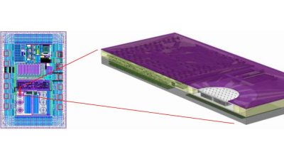
The OV02E is compact, and suitable for devices with a screen-to-body ratio of less than 3mm Y size, such as tablets and wearable devices. It has a 1.12 micron backside illuminated (BSI) pixel based on Omnivision’s proprietary PureCel Plus architecture for advanced pixel sensitivity and quantum efficiency. The sensor features 2Mpixel, full HD 1080p video at 60 frames per second and supports multiple camera synchronisation for machine vision and IoT applications which require depth detection. The OV02E sensor’s always-on capability has a low power state that works with the mobile industry processor interface (MIPI) and serial peripheral interface (SPI).

Samples of the OV02E are available now, and it will be in mass production in Q4 2023. 

Omnivision is a fabless semiconductor company which develops advanced digital imaging, analogue and touch and display solutions for multiple applications and industries, including mobile phones, security and surveillance, automotive, computing, medical and emerging applications. 

http://www.ovt.com

> Read More

Nanusens shrinks sensor and control circuit for ASICs with embedded sensors

By simultaneously shrinking the sensor and control circuit, Nanusens has created a digital circuit design to measure the capacitance of its nanosensors to create ASICs with integrated sensors. Both the sensor structure and its detection circuitry can be made at the same time within a chip using standard CMOS processes on whatever process node is required, explained the company. As a result, ASICs can now be made with several sensors embedded within them. Integrating sensors as IP blocks offers dramatic reductions in costs and size, claimed Nanusens, as it completely replaces the current solution of discrete sensor packages.

“This is a major milestone for the company,” said Dr. Josep Montanyà, CEO of Nanusens. “The first was successfully making our unique, nanoscale, sensor structures within the CMOS layers. This solves the problem that conventional MEMS have to be made on custom production lines that have limited production capabilities whereas we can make almost unlimited numbers of our sensors in CMOS fabs. These are available in standard packages such as LGA, QFN, WLCSP and others, but, like all other MEMS sensors, they require analogue circuitry to detect tiny capacitance changes coming from nano-displacements of their devices in operation. Our breakthrough is the creation of a fully digital detection circuit as this can be scaled down to the process node being used for the sensor structure and pairs to form a complete sensor and detection solution.

Shrinking the sensor and circuitry simultaneously enables the company to take advantage of smaller CMOS geometries which include reduced costs and reduced power consumption of more than 10 times compared to analogue detection circuits. “This is impossible for other MEMS sensor solutions as their structures cannot be shrunk neither can their analogue circuits as their transistors need a large area to maintain the required low levels of noise,” said Montanyà.

The all-digital detection circuit provides a very fast on / off switching of the circuit of three microseconds compared to 300 microseconds or several milliseconds in conventional analogue transconductance / charge amplifier or similar circuits, said Nanusens. This is advantageous for applications which require a low sampling frequency, such as motion detector applications where the motion detector is typically used to wake up the rest of the device. If the device is in sleep mode most of the time, the battery life is dependent on the current consumption of the motion detector. The fast on / off of the new digital detection circuit results in sub micro A current consumption on the 180nm test chip, which more than doubles the battery life in these applications.

“Instead of being discrete packages on a PCB or a multi-die solution, all the required sensors can be integrated into an ASIC just like another IP block,” said Montanyà. Portable multi-sensor devices, such as smart phones, ear buds and smart watches will benefit from the reduction in BoM, size and power budget and Nanusens confirmed that it is in discussion with companies who want to license this IP.

Founded in 2014, Nanusens is headquartered in Paignton, Devon, England with R & D offices in Barcelona, Spain and Shenzen, China. 

http://www.nanusens.com

> Read More

SigmaSense partners with NXP Semiconductors for future sensing systems

Texas company, Sigma Sense has developed a sensing technology which it says will improve the performance of practically anything with a touchscreen, for example mobile phones, automotive, industrial, gaming, wearables, digital signage, industrial / IoT and even improve the performance of EV batteries.

SigmaSense’s technology intends to ‘shake up’ the industry in which the underlying technology behind most of today’s touch sensing devices has changed little in decades.

It said its approach captures more granular data from the physical world making interactive advances possible. The technology makes possible high speed touch interfaces of all sizes and shapes, new surface materials beyond glass, operation in rain and with gloves, economical large format interactive displays with the speed of a mobile experience.  

SigmaSense has announced a license and co-development deal with NXP Semiconductors to transition from traditional touch interfaces to multi-dimensional sensing. It has licensed its technology to NXP, and the companies will collaborate on high-performance sensing products for specific applications, in particular those with demands for faster, more robust, fully immersive software-defined experiences.

 “The next generation of smart devices and applications are demanding data for enhanced functionality that requires an entirely new software-programmable approach to sensing,” explained Lars Reger, CTO of NXP Semiconductors.

Rick Seger, CEO of SigmaSense, added: “Our co-development with NXP marks the transition to a universe of new data-centric design options driven by software-defined sensing.”

SigmaSense’s multi-dimensional sensing works through many different surfaces, shapes, and materials, enabling previously impossible designs. It makes it possible to extract “vastly more” data from the physical world for a wide range of products and systems, said the company. With the ability to measure current direct-to-digital, SigmaSense claimed to deliver  an industry first of low voltage, frequency domain sensing. Fast, continuous, high-fidelity data capture with intelligent digital signal processing moves analogue challenges to the digital domain, where design flexibility can deliver orders of magnitude improvement, continued SigmaSense. The technology has the potential to change system designs “from foldable displays to EV batteries,” said the company.

SigmaSense invented software-defined sensing which achieves breakthrough levels of speed, accuracy, resolution, and noise immunity previously deemed impossible for sensing systems. Sensing through the noise, SigmaSense products increase the depth and quantity of data that can be captured from the physical world to enable exciting new experiences in a wide range of devices including mobile, automotive, battery sensing, digital signage, wearables, and all sizes of IoT touch displays. 

SigmaSense is headquartered in Austin, Texas, USA, with offices in Boise, Idaho and Taipei, Taiwan.

https://sigmasense.com

> Read More

Sensor uses motion and bone conduction to save space and power

Headsets and hearable devices can be reduced in size and power budget using the STMicroelectronics’ motion and bone-conduction sensor, said the company. The LSM6DV16BX can deliver a longer listening experience and superior hearing in TWS (true wireless stereo) headphones and AR / VR / MR headsets.
The integrated sensors can save space inside hearable devices including sports and general-purpose earbuds. It combines a six-axis inertial measurement unit (IMU) for head tracking and activity detection with an audio accelerometer for detecting voice through bone conduction in a frequency range that exceeds 1kHz.

The LSM6DSV16BX contains ST’s Qvar charge-variation detection technology for user-interface controls such as touching and swiping.
The LSM6DSV16BX sensor embeds ST’s Sensor Fusion Low Power (SFLP) technology, specifically designed for head tracking and 3D sound, and the in-the-edge processing resources featured in ST’s third generation MEMS sensors, including finite state machine (FSM) for gesture recognition, the machine learning core (MLC) for activity recognition and voice detection, and adaptive self-configuration (ASC), which automatically optimises performance and efficiency. These help to reduce system latency while saving overall power and offloading the host processor.
The enhanced integration and edge processing save up to 70 per cent of system power consumption and 45 per cent of PCB area. In addition, the number of pin connections can be reduced by 50 per cent, saving external connections, and the package height is 14 per cent less than earlier MEMS inertial sensors from ST.
The LSM6DSV16BX comes with many software examples, available on ST MEMS GitHub FSM and MLC model zoo. These include pick-up gesture detection to automatically turn on some device’s services, in-ear and out-of-ear detection in TWS headsets and head gestures for 3D sound in headphones. To save developer time, without starting from scratch, pre-integrated application examples are available in X-Cube-MEMS1 package.
The LSM6DSV16BX is in production now, available in a 2.5 x 3.0 x 0.74mm VFLGA package.


http://www.st.com/

> Read More

About Smart Cities

This news story is brought to you by smartcitieselectronics.com, the specialist site dedicated to delivering information about what’s new in the Smart City Electronics industry, with daily news updates, new products and industry news. To stay up-to-date, register to receive our weekly newsletters and keep yourself informed on the latest technology news and new products from around the globe. Simply click this link to register here: Smart Cities Registration