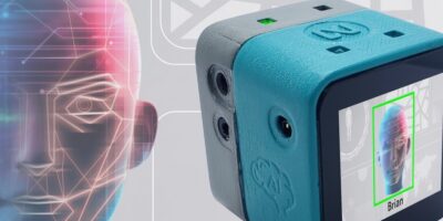
Reference IP accelerates creation of signal and data processing SoCs

Power signal and data processing SoCs can be created faster and for lower costs, says Sondrel, using its latest reference IP platform.

The SFA 300 reference IP is the latest addition to the. It is a semi-custom SoC design to which a customer’s IP can be added to create a bespoke solution for high performance data processing.

Each SFA 300 reference design has four CPU clusters. Several SFA 300s can be ganged together and synchronised via the PCIe interface to scale the processing performance. There is also the option to integrate accelerators and/or custom logic to further increase performance and minimise power requirements. Developers can use the SFA 300 to tailor designs for processing-intense applications such as 8K video, artificial intelligence (AI), facial recognition for surveillance, smart factories, blockchain servers and medical data analysis.

An ASIC with four CPU clusters is complex to design,” explained Rowan Naylor, a principal engineering consultant at Sondrel. “Moving data around the chip without bottlenecks needs a network on chip, a multi-width data path, internal RAM, scaled and distributed across the design for optimal performance, and data conflict arbitration”. He also went on to explain that data security aspects are required in the Arm-based security sub-system, such as activity/intrusion detection. These function are in the SFA 300 IP platform, which allows engineers to reduce the design time and costs by up to 30 per cent, declared Naylor.

The SFA 300 framework design enables it to be scaled to suit the application as well as be the basis for different solutions of varied processing power capabilities. The four CPUs can be chosen to suit the processing power need by each of the four channels of the chip because the interconnects on and off the CPUs are standardised. This standardisation of interconnects on the boundaries of IP blocks and the rest of chip enables most other IP blocks such as memory to be also exchanged as required.

If the processing power required is greater than can be achieved by upgrading the processors, then several chips can be ganged together to form a cluster to achieve the processing power required with the limiting factor being the speed of inter-chip communications dropping as more chips are ganged together.

According to Sondrel, this is an inexpensive means of achieving a high-performance solution as it requires just one chip repeated several times rather than a more expensive, single chip solution. Typical performance figures are 4 tera operations per second (TOPS) for each channel for AI and 400 giga operations per second for each channel for DSP.

The SFA 300 can be used for image and video analysis, for example. For a static image, it could find a face or count the number of blood cells on a sample slide and a neural net could provide more sophisticated recognition for data analysis, explained the company. Treating a video as a series of images, it could deduce the direction and speed of an object of interest.

Another use case could be heavy duty number crunching such as for block chains and cryptocurrency mining.

The SPA 300 has low power consumption, making it suitable for battery powered applications, such as a drone. The powerful image processing capabilities and AI enable it to be used as an autonomous drone controller to fly the drone.

The SPA 300 is the third in the company’s Architecting the future IP platforms.

Sondrel offers a full turnkey service that turns designs into fully tested, shipping silicon.

http://www.sondrel.com

> Read More

Mouser Electronics signs global distribution deal with QuickLogic

Embedded FPGA IP, low power, multi-core, voice-enabled SoCs and endpoint artificial intelligence (AI) from Quicklogic is now available from Mouser Electronics, following a global distribution agreement between the developers and the distributor.

The agreement means that Mouser now stocks QuickLogic’s EOS S3 microcontroller- and FPGA-based platform and its QuickFeather development kit.

The EOS S3 sensor processing platform is a multi-core SoC that enables an array of concurrent sensor applications, from basic to computationally demanding algorithms for smartphone, wearable, and IoT devices. EOS S3 integrates a low-power Arm Cortex-M4F microcontroller sub system and embedded FPGA (eFPGA) fabric, with optional sensory low power sound detect (LPSD) for on-chip voice recognition. The heterogeneous architecture enables designers to partition their software and use cases across the variety of cores to optimise a system for lowest power consumption.

The QuickFeather development kit is a small form factor system which enables the next generation of low power machine learning (ML) -capable IoT devices, explains Mouser. It is powered by the EOS S3 and is based on open source hardware. It is compatible with the Adafruit Feather form factor. The board is built around an open source software ecosystem, including SymbiFlow FPGA tools, Zephyr and FreeRTOS operating systems and Renode. Third-party software is available for sensor processing, voice, and AI/ML use cases, including SensiML and Google’s TensorFlow Lite for microcontrollers.

Mouser is a global authorised distributor, offering a wide selection of the newest semiconductors and electronic components which are in stock and ready to ship. To help speed customers’ designs, Mouser’s website hosts an extensive library of technical resources, including a Technical Resource Centre, along with product data sheets, supplier-specific reference designs, application notes, technical design information, engineering tools and other helpful information.

Mouser Electronics’ website is available in multiple languages and currencies and features more than five million products from over 1,100 manufacturer brands. Mouser offers 27 support locations worldwide and ships to 223 countries/territories from its distribution facilities in the Dallas, Texas, metro area in the US.

http://eu.mouser.com

> Read More

Bluetooth 5.0 for RE microcontroller uses SOTB for energy harvesting

The latest member of Renesas Electronics’ RE family of microcontroller is the RE01B, which has Bluetooth 5.0 support. The 32-bit low power microcontroller was developed using Renesas’ SOTB (Silicon on Thin Buried Oxide) process technology.

The Bluetooth-capable RE01B is suitable for energy harvesting systems and intelligent IoT devices that operate constantly at extremely low power levels without having to replace or recharge batteries. The RE01B microcontroller makes it easier to implement regular data management and firmware updates over Bluetooth while maintaining low power consumption, which extends the battery life.

The on-chip energy harvesting control circuit (rapid start up capacitor charging and secondary battery charge protection functionality) allows users to achieve battery-less Bluetooth communication. Energy harvesting and power storage can be directly connected to the RE01B.

The microcontroller is suitable for compact healthcare devices such as pulse oximeters and biomedical sensor patches, remote controls with voice recognition capabilities and smart meter modules. RE01B can also be used for IoT devices that require constant operation, period data collection and updates, such as devices for monitoring the elderly, children or assets in transit.

The RE01B is built around the Arm Cortex-M0+ core and Renesas’ proprietary SOTB process technology. It operates at a maximum operating frequency of 64MHz and achieves current consumption as low as 35 microA/MHz during operation and 600nA during standby; this is among the lowest in the industry for a Bluetooth-capable microcontroller, says Renesas. It can also be combined with Renesas’ ISL9123 ultra-low Iq DC/DC converter, configured as an external step-down regulator, to reduce current consumption during operation down to 15 microA/MHz to improve power efficiency.

It has 1.5Mbyte flash memory and 256Kbyte SRAM with Bluetooth functionality, suitable for over the air (OTA) firmware updating.

The RE01B is in a 64-pin QFN package measuring 8.0 x 8.0mm.

Security function include Trusted Secure IP and Renesas offers application programming interfaces (APIs) conforming to standard protocols, such as heart rate profile (HRP), environment sensing profile (ESP), and automation I/O profile (AIOP), in addition to Bluetooth 5.0 protocol stack.

Development tools for the RE family, include a QE for Bluetooth Low Energy, which generates programs for custom Bluetooth profiles that can then be integrated into the user’s own application programs, and a Bluetooth test tool suite, which provides a graphical user interface that allows users to perform initial wireless characteristics evaluations and Bluetooth functionality verification.

The RE01B is available now. The EB-RE01B evaluation kit from Tessera Technology is also available now.

http://www.renesas.com

> Read More

ST extends STM32WB series with extra power-saving modes

Devices that combine entry-level features with extra power savings have been added to the STM32WB Bluetooth Low Energy microcontroller series.

The dual-core STM32WB15 and STM32WB10 Value Line pair an Arm Cortex-M4 processor, which runs the main application with a Cortex-M0+ for Bluetooth 5.2 connectivity. ST explains that this ensure real-time performance from each. The radio stage has a 102dBm link budget to ensure reliable connections over long distances and integrates balun circuitry to save board space and reduce the bill of materials.

The STM32WB15 and STM32WB10 have a power saving mode that allows the radio to remain operational. They also have tailored peripherals and memory to suit cost-sensitive, power-conscious embedded applications including wearables, beacons, smart circuit breakers, trackers, IoT endpoints, and equipment for industrial automation.

There is a software development kit (SDK) for each microcontroller. This includes standardised radio protocol stacks and openness to proprietary protocols with a set of security mechanisms that ensure safe software updates for device integrity. There is also Proprietary Code Read-Out Protection (PCROP) to guard intellectual property.

The STM32WB series scales across package variants, offering options such as extended general purpose I/Os and pin-to-pin compatibility between similar packages of the portfolio. Customers can migrate designs between devices to take advantage of different features and memory densities.

The development ecosystem includes STM32Cube-certified radio stacks, software expansion packs and sample code, the STM32CubeMX configurator and initialisation code generator, the STM32CubeIDE development environment, a powerful STM32CubeMonitor-RF evaluation tool, and associated Nucleo hardware tools.

The STM32WB15 and STM32WB10 microcontrollers are in production now, offering various pin-compatible configurations in a QFN48 package.

http://www.st.com

> Read More

About Smart Cities

This news story is brought to you by smartcitieselectronics.com, the specialist site dedicated to delivering information about what’s new in the Smart City Electronics industry, with daily news updates, new products and industry news. To stay up-to-date, register to receive our weekly newsletters and keep yourself informed on the latest technology news and new products from around the globe. Simply click this link to register here: Smart Cities Registration