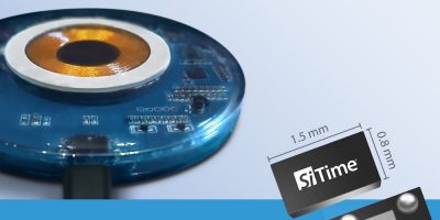
Nordic introduces first PMIC for tight spaces

Nordic Semiconductor’s first power management device is the nPM1100, a power management integrated circuit (PMIC). It combines a USB compatible Li-ion/Li-Po battery charger and DC/DC buck regulator in a compact WLCSP for space-constrained applications.

The low IQ PMIC for the company’s nRF52/nRF53 series SoCs and other compatible devices. The 400mA battery charger and 150mA DC/DC step down regulator is integrated with a USB-compatible input regulator with overvoltage protection in a WLCSP which measures 2.075 x 2.075mm. The PMIC ensures reliable power supply and stable operation for the nRF52 and nRF53 series multi-protocol SoCs and maximises the application battery life, says Nordic. It can be used as a generic PMIC for any application using rechargeable Lithium Ion or Lithium Polymer batteries.  Its form factor makes it suitable for wearables, connected medical devices, and other space-constrained applications.

The nPM1100’s battery charger can bypass the first regulator stage of Bluetooth Low Energy (BLE) applications based on nRF52 and nRF53 SoCs. In this configuration the buck regulator’s high efficiency reduces overall system power consumption while its 150mA current capability increases the current available for other system components from approximately 10 to 100mA.

The nPM1100 features a low quiescent current (IQ) of 700nA (typicall) which can be further reduced to 470nA in “ship mode” (i.e disabling the power output, removing the need for an external power switch), which minimises battery lifetime impact on products in transit. The power management solution takes up as little as 23mm2 of PCB area, including passive components (rising to 27mm2 when optimised for performance).

The nPM1100 input regulator draws its power from either a 4.1 to 6.6V USB input or from a 2.3 to 4.35V connected battery input. It can supply a 3.0 to 5.5V unregulated voltage to the application at up to 500mA output current. The PMIC supports USB standard downstream port (SDP), charging downstream port (CDP) and dedicated charger port (DCP) detection. The input regulator includes over-voltage protection for transient voltage spikes up to 20V.

The battery charger is JEITA-compliant and will charge the application’s Li-ion/Li-Po battery with a resistor-selectable charge current from 20 to 400mA and a selectable termination voltage of 4.1 or 4.2V. The charger includes battery thermal protection and automatic selection from three charging modes: automatic trickle, constant current and constant voltage. The charger also features a discharge current limitation.

The DC/DC buck voltage regulator runs at more than 90 per cent efficiency down to below 100 microA load current. It takes its power from the input system regulator and provides up to 150mA current at a selectable 1.8, 2.0, 2.7 or 3.0V regulated output voltage. The regulator features soft start up and automatic transition between hysteretic and pulse width modulation (PWM) modes. It also supports a forced PWM mode for clean power operation.

No configuration software is required as all settings are pin configurable. The PMIC is compatible with all devices designed to operate within the output voltages and supply currents the chip can deliver. The product’s operating temperature range is -40 to 85 degrees C.

Nordic also offers the nPM1100 evaluation kit with switches for all selectable settings, buttons to enter and exit ship mode and connectors for batteries, USB and headers for all pins on the PMIC. It can be powered by USB via the on-board micro-USB port, from an external DC power supply through header pins or from battery power via the battery connectors on one of the headers.

http://www.nordicsemi.com

> Read More

IP suite and Armv9 Cortex CPUs are part of Arm’s Total Compute

Arm has created Total Compute solutions, assembling hardware IP, physical IP, software, tools and standards based the recently introduced Armv9 architecture.

There are Armv9 CPU cores designed for consumer devices, including laptops, smart TVs, and mobile gaming. Arm Cortex-X2 is Arm’s most powerful CPU to date, delivering 30 per cent performance improvements compared with today’s flagship Android smartphones, says the company. It is also scalable across smartphones and laptops.

Arm Cortex-A710 is also based on Armv9 and has a 30 per cent energy efficiency gain and 10 per cent uplift in performance compared to the Cortex-A78.

Another announcement is the Arm Cortex-A510, which delivers 35 per cent performance improvements and increases machine learning (ML) performance, for use in smartphone, home and wearable devices.

Described as the backbone of the Armv9-A CPU cluster is a new DynamIQ Shared Unit, the DSU-110, which is scalable and supports up to eight Cortex-X2 CPUs, together with security and ML features.

Arm also announced that all cores for mobile applications will be 64-bit only by 2023, with support for all apps from Arm’s partners worldwide.

The latest CoreLink CI-700 Coherent Interconnect and CoreLink NI-700 Network-on-Chip Interconnect work seamlessly with Arm CPU, GPU and NPU IP to enable system enhancements. CoreLink CI-700 and CoreLink NI-700 have hardware level support for Armv9-A features, such as memory tagging extension (MTE), and support increased security, improved bandwidth and latency.

http://www.arm.com

> Read More

Reference IP accelerates creation of signal and data processing SoCs

Power signal and data processing SoCs can be created faster and for lower costs, says Sondrel, using its latest reference IP platform.

The SFA 300 reference IP is the latest addition to the. It is a semi-custom SoC design to which a customer’s IP can be added to create a bespoke solution for high performance data processing.

Each SFA 300 reference design has four CPU clusters. Several SFA 300s can be ganged together and synchronised via the PCIe interface to scale the processing performance. There is also the option to integrate accelerators and/or custom logic to further increase performance and minimise power requirements. Developers can use the SFA 300 to tailor designs for processing-intense applications such as 8K video, artificial intelligence (AI), facial recognition for surveillance, smart factories, blockchain servers and medical data analysis.

An ASIC with four CPU clusters is complex to design,” explained Rowan Naylor, a principal engineering consultant at Sondrel. “Moving data around the chip without bottlenecks needs a network on chip, a multi-width data path, internal RAM, scaled and distributed across the design for optimal performance, and data conflict arbitration”. He also went on to explain that data security aspects are required in the Arm-based security sub-system, such as activity/intrusion detection. These function are in the SFA 300 IP platform, which allows engineers to reduce the design time and costs by up to 30 per cent, declared Naylor.

The SFA 300 framework design enables it to be scaled to suit the application as well as be the basis for different solutions of varied processing power capabilities. The four CPUs can be chosen to suit the processing power need by each of the four channels of the chip because the interconnects on and off the CPUs are standardised. This standardisation of interconnects on the boundaries of IP blocks and the rest of chip enables most other IP blocks such as memory to be also exchanged as required.

If the processing power required is greater than can be achieved by upgrading the processors, then several chips can be ganged together to form a cluster to achieve the processing power required with the limiting factor being the speed of inter-chip communications dropping as more chips are ganged together.

According to Sondrel, this is an inexpensive means of achieving a high-performance solution as it requires just one chip repeated several times rather than a more expensive, single chip solution. Typical performance figures are 4 tera operations per second (TOPS) for each channel for AI and 400 giga operations per second for each channel for DSP.

The SFA 300 can be used for image and video analysis, for example. For a static image, it could find a face or count the number of blood cells on a sample slide and a neural net could provide more sophisticated recognition for data analysis, explained the company. Treating a video as a series of images, it could deduce the direction and speed of an object of interest.

Another use case could be heavy duty number crunching such as for block chains and cryptocurrency mining.

The SPA 300 has low power consumption, making it suitable for battery powered applications, such as a drone. The powerful image processing capabilities and AI enable it to be used as an autonomous drone controller to fly the drone.

The SPA 300 is the third in the company’s Architecting the future IP platforms.

Sondrel offers a full turnkey service that turns designs into fully tested, shipping silicon.

http://www.sondrel.com

> Read More

Mouser Electronics signs global distribution deal with QuickLogic

Embedded FPGA IP, low power, multi-core, voice-enabled SoCs and endpoint artificial intelligence (AI) from Quicklogic is now available from Mouser Electronics, following a global distribution agreement between the developers and the distributor.

The agreement means that Mouser now stocks QuickLogic’s EOS S3 microcontroller- and FPGA-based platform and its QuickFeather development kit.

The EOS S3 sensor processing platform is a multi-core SoC that enables an array of concurrent sensor applications, from basic to computationally demanding algorithms for smartphone, wearable, and IoT devices. EOS S3 integrates a low-power Arm Cortex-M4F microcontroller sub system and embedded FPGA (eFPGA) fabric, with optional sensory low power sound detect (LPSD) for on-chip voice recognition. The heterogeneous architecture enables designers to partition their software and use cases across the variety of cores to optimise a system for lowest power consumption.

The QuickFeather development kit is a small form factor system which enables the next generation of low power machine learning (ML) -capable IoT devices, explains Mouser. It is powered by the EOS S3 and is based on open source hardware. It is compatible with the Adafruit Feather form factor. The board is built around an open source software ecosystem, including SymbiFlow FPGA tools, Zephyr and FreeRTOS operating systems and Renode. Third-party software is available for sensor processing, voice, and AI/ML use cases, including SensiML and Google’s TensorFlow Lite for microcontrollers.

Mouser is a global authorised distributor, offering a wide selection of the newest semiconductors and electronic components which are in stock and ready to ship. To help speed customers’ designs, Mouser’s website hosts an extensive library of technical resources, including a Technical Resource Centre, along with product data sheets, supplier-specific reference designs, application notes, technical design information, engineering tools and other helpful information.

Mouser Electronics’ website is available in multiple languages and currencies and features more than five million products from over 1,100 manufacturer brands. Mouser offers 27 support locations worldwide and ships to 223 countries/territories from its distribution facilities in the Dallas, Texas, metro area in the US.

http://eu.mouser.com

> Read More

About Smart Cities

This news story is brought to you by smartcitieselectronics.com, the specialist site dedicated to delivering information about what’s new in the Smart City Electronics industry, with daily news updates, new products and industry news. To stay up-to-date, register to receive our weekly newsletters and keep yourself informed on the latest technology news and new products from around the globe. Simply click this link to register here: Smart Cities Registration