Secora Pay on 40nm process offers new applets contactless payments

Contactless payment has been gaining in popularity and Infineon says its Secora Pay portfolio on 40 nm technology addresses many of the new payment card and devices. It uses the company’s Solid Flash chip and offers new applets and customised value-added products for standard payment cards (Secora Pay S) as well as multi-application cards (Secora Pay X) and components to turn any device into a payment device (Secora Pay W).

The product portfolio also provides applets of global (Visa, MasterCard, Discover, and American Express) and domestic networks. It offers state-of-the-art contactless and personalization performance, allowing MasterCard contactless transactions of 200ms.

Secora Pay options on 40 nm technology offer backward compatibility to existing Secora Pay products in terms of card production antenna designs, personalisation and product certification. The family uses a security controller including certified software integrated in coil on module (CoM) chip modules and fine-tuned inlays for seamless card production.

Infineon uses inductive coupling technology and wire embedded card antennas for the CoM system which is claimed to offer high flexibility in card designs. It can be integrated into environmentally friendly cards from recycled and ocean-bound plastic or wood, high performance dual interface metal or LED cards, says Infineon.

According to Infineon, Secora Pay products support the highest throughput in card production with minimum consumable material for manufacturing highly robust dual interface cards. As well as saving resources, new value added services based on Secora Pay’s NFC tag functionality are offered, allowing additional use cases like initial card activation.

The pre-certified Secora Pay W with SPA2.1, a small antenna on 35 mm film tape, addresses the growing demand for payment accessories and new payment form factors. In combination with payment and tokenisation services provided by partners, Infineon explains that it allows the easy integration of payment functionality into end-customer applications, for convenient contactless payment functionalities for wearables like wristbands as well as key fobs or other form factors.

Product versions supporting the latest Visa and MasterCard applications are available now. Additionally, applets supporting American Express, Discover and others will become available in Q1/2022.

http://www.infineon.com

> Read More

Renesas bases RA2E2 microcontroller family on Arm Cortex-M23 core

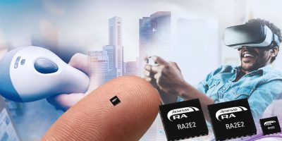
For small and energy-sensitive IoT, wearable, medical, industrial automation, consumer and home appliance applications, Renesas offers the RA2E2 microcontroller group. It is based on the Arm Coretex-M23 core and is the latest addition to the 32-bit RA family.

The family of microcontrollers is claimed to offers a combination of low power consumption, a set of peripherals targeted at IoT endpoint applications and space-saving packaging options including a tiny 16-pin WLCSP (wafer level chip scale package) measuring only 1.87 x 1.84mm. The 48MHz RA2E2 family is claimed to offer the industry’s lowest operating power in their class, consuming only 81microA/MHz in active mode with software standby current of only 200nA with fast wake up. They also support a wide temperature range of Ta = -40/+125 degrees C for harsh IoT operating environments. The RA2E2 microcontrollers support an I3C bus interface and integrate cost-saving peripheral functions, including an on-chip oscillator with precision of +/- one per cent, power on reset, low voltage detector, EEPROM and a temperature sensor.

The RA2E2 Group includes nine devices, spanning from 16- to 24-pin packages, and from 16 to 64kbyte of flash memory and 8kbyte of SRAM. The devices also include 2kbyte of data flash memory, which is atypical in low-pin count devices, says Renesas. They are also claimed to be the only microcontrollers in their class to offer an I3C bus interface, delivering high-speed communications of 4.6Mbits per second while significantly reducing power consumption. Security features include a cryptography accelerator (AES256/128), a true random number generator (TRNG) and memory protection units.

The RA2E2 group is available today. Renesas is also offering the EK-RA2E2 evaluation kit.

The Renesas RA family includes over 160 parts ranging from 48 to 200MHz. They have a wide range of communications and security options, including Arm TrustZone technology. All RA devices are supported by the Renesas Flexible Software Program (FSP) that includes drivers and middleware to ease the implementation of communications and security. The FSP’s graphical user interface (GUI) simplifies and accelerates the development process, says Renesas. It enables flexible use of legacy code as well as easy compatibility and scalability with other RA devices. Designers using FSP also have access to the Arm ecosystem and tools as well as Renesas’ partner network.

http://www.renesas.com

> Read More

Intel expands neuromorphic research chip – introducing Loihi 2

Now with one million neurons, the second generation research chip from Intel, Loihi 2, uses a pre-production Intel 4 process. There is also now a software framework for developing neuro-inspired applications.

The second-generation chip improves the speed, programmability, and capacity of neuromorphic processing, comments Mike Davies, director of Intel’s Neuromorphic Computing Lab. Loihi 2 broaden the processing technology’s use in power and latency constrained intelligent computing applications. “We are open sourcing Lava to address the need for software convergence, benchmarking, and cross-platform collaboration in the field, and to accelerate our progress toward commercial viability,” adds Davies.

Neuromorphic computing draws insights from neuroscience to create chips that function more like the biological brain. Researchers hope that it will deliver orders of magnitude improvements in energy efficiency, speed of computation and efficiency of learning across edge applications including vision, voice and gesture recognition to search retrieval, robotics, and constrained optimisation problems. To this end, Intel and partners have demonstrated robotic arms, neuromorphic skins and olfactory sensing projects.

Advances in Loihi 2 allow the architecture to support new classes of neuro-inspired algorithms and applications and provide processing that is 10 times faster than its predecessor. It also exhibits up to 15 times greater resource density (up to one million neurons per chip), and improved energy efficiency.

Fabricated with a pre-production version of the Intel 4 process, the use of extreme ultraviolet (EUV) lithography has simplified the layout design rules compared to past process technologies for rapid development of Loihi 2, says Intel.

The Lava software is an open, modular, and extensible framework, for researchers and application developers to build on each other’s progress and converge on a common set of tools, methods, and libraries. Lava runs seamlessly on heterogeneous architectures across conventional and neuromorphic processors, and is interoperable with a variety of AI, neuromorphic and robotics frameworks.

Developers can begin building neuromorphic applications without access to specialized neuromorphic hardware and can contribute to the Lava code base, including porting it to run on other platforms.

Loihi 2’s greater programmability will allow a wider class of difficult optimisation problems to be supported, including real-time optimisation, planning, and decision-making from edge to data centre systems.

Loihi 2 also improves support for advanced learning methods, including variations of backpropagation, the algorithm of deep learning.

Fully programmable neuron models and generalised spike messaging in Loihi 2 suggest reductions of over 60 times fewer ops per inference compared to standard deep networks running on the original Loihi without loss in accuracy. It incorporates faster, more flexible, and more standard I/O interfaces, including Ethernet interfaces, glueless integration with a wider range of event-based vision sensors, and larger meshed networks of Loihi 2 chips.

http://www.intel.com

> Read More

Wireless charging transmitter coil driver is in QFN3x3 package

The first in a family of coil drivers from Alpha and Omega Semiconductor (AOS) that are supplied in a thermally enhanced QFN3x3 package are suitable for wireless charging transmitter circuits in a variety of space constrained applications.

The AOZ32033AQI is an integrated half-bridge gate driver capable of driving high-side and low-side N-channel MOSFETs. The coil driver offers 30V, 11 mOhm in a QFN3x3 package. It features slew rate control (SRC) to adjust sink / source current and provide a trade-off between efficiency and EMI optimisation in the design of wireless charging transmitter (TX) circuits, explains AOS.

The coil driver is intended for use in wireless charging TX circuits used in cordless power tools, vacuum cleaners, drones, and other consumers’ electronic equipment which use full-bridge topology with a resonant tank circuit for power conversion efficiency.

The integrated package offers a part count reduction of up to 40 per cent compared to traditional approaches, says AOS. The AOZ32033AQI enables PCB space savings and higher performance in wireless transmitter circuits with high wattage of up to 30W. To ensure the design is robust, the coil driver has multiple protection functions such as high side and low side under-voltage lockout and over-temperature protection. The coil driver can be used for a wide range of input voltages from 4.0 to 28V.

“Wireless charging is offered at increasingly higher power levels as the benefits of eliminating physical connectors and cables are being realised by more end applications,” says said Colin Huang, power IC marketing manager at AOS. This, the first member announced of the company’s coil driver product family, will provide an efficient, power-dense, and cost-effective solution for wireless charging TX circuits, he continues. “The integrated approach offers protection features not possible by using a discrete approach while reducing engineering design cycles and complexities,” he says.

The AOZ32033AQI is immediately available in production quantities with a lead-time of 12 weeks.

Alpha and Omega Semiconductor (AOS) is a designer, developer, and global supplier of a broad range of power semiconductors, including a wide portfolio of  power MOSFET, IGBT, IPM, TVS, HVIC, SiC/GaN, power IC, and digital power products. AOS has developed extensive IP and technical knowledge to introduce innovative products to address the increasingly complex power requirements of advanced electronics.

AOS’s portfolio of products targets high-volume applications, including portable computers, flat-panel TVs, LED lighting, smartphones, battery packs, consumer and industrial motor controls, automotive electronics, and power supplies for TVs, computers, servers, and telecommunications equipment.

http://www.aosmd.com

> Read More

About Smart Cities

This news story is brought to you by smartcitieselectronics.com, the specialist site dedicated to delivering information about what’s new in the Smart City Electronics industry, with daily news updates, new products and industry news. To stay up-to-date, register to receive our weekly newsletters and keep yourself informed on the latest technology news and new products from around the globe. Simply click this link to register here: Smart Cities Registration