MEMS sensors add machine learning in the edge and electrostatic sensing 

A third generation of MEMS sensors are intended for consumer mobiles and smart industries, healthcare, and retail.

MEMS technology drives the intuitive context-aware features of today’s smartphones and wearables. STMicroelectronics claims that its latest generation of MEMS sensors take performance beyond established technical limitations on output accuracy and power consumption. The new sensors can deliver the highest accuracy for product features such as activity detection, indoor navigation, and precision industrial sensing. At the same time, they keep battery demand low for longer runtimes.

Selected variants include extra features such as ST’s machine learning core (MLC) and electrostatic sensing. The MLC brings adaptive, machine learning capabilities to edge applications that operate at extremely low power. The charge variation (QVAR) sensing channel monitors changes in electrostatic charge, either through contact with the body in a smartwatch or fitness band or by non-contact sensing (radar). The MEMS sensors with QVAR can enhance user interface controls for seamless interactions or to simplify detection of moisture and condensation. Radar mode applications include human presence detection, activity monitoring and people counting.

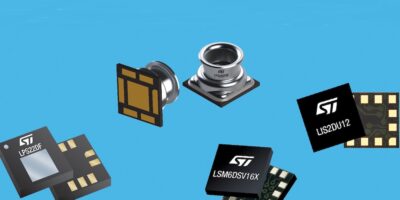
The LPS22DF and waterproof LPS28DFW barometric pressure sensors operate from 1.7 microA and have absolute pressure accuracy of 0.5hPa. The LPS28DFW has dual full scale capability, enabling accurate vertical position both underwater and out of water. The full scale range is selectable up to 1260 or 4060hPa, equivalent to water pressure at a depth of about 98 feet (30m). The sensors enhance altimeter and barometer performance in portable devices and wearables including sport watches. Typical industrial applications include equipment for weather monitoring and accurate water-depth sensing.

The LIS2DU12 three-axis accelerometer has been designed to build a low power architecture with active anti-aliasing. The anti-aliasing filter operates with a current consumption among the lowest in the market, claims STMicroelectronics. The LIS2DU12 consumes only 3.5 microA at 100Hz output data rate (ODR) and is also the first accelerometer with I3C interface, according to the company. 

The accelerometer is a small footprint of 2.0 x 2.0 x 0.74mm. The accelerometer is designed for wearable devices, hearing aids, true wireless stereo (TWS) and wireless sensor nodes.

The LSM6DSV16X six-axis iNEMO inertial module contains QVAR electrostatic sensing as well as the MLC and a finite state machine (FSM). The operating current can be as little as 12 microA. The FSM enables adaptive self-configuration (ASC). With ASC, the device understands the context and reconfigures itself without waking up the system, gaining a significant extra power saving. 

The MEMS sensor will enter production and has been demonstrated in an electrostatic radar application for early user detection to accelerate waking-up a laptop PC.

The LPS22DF pressure sensor is supplied in a 2.0 x 2.0 x 0.73mm 10-lead LGA package and the LPS28DFW is supplied in a 2.8 x 2.8 x 1.95mm seven-lead LGA are in production now. Free samples are available. The LIS2DU12 and LSM6DSV16X are scheduled for production later in 2022.

http://www.st.com

> Read More

SoC uses computing-in-memory for speech processing at the edge

Computing-in-memory technology is poised to eliminate the massive data communications bottlenecks associated with AI speech processing at the network’s edge, said Witinmen. The company has worked with Microchip Technology’s subsidiary Silicon Storage Technology (SST) to develop an embedded memory that simultaneously performs neural network computation and stores weights. Microchip Technology announced that its SuperFlash memBrain neuromorphic memory has been combined with the Witinmem neural processing SoC. The SoC is claimed to be the first in volume production that enables sub-mA systems to reduce speech noise and recognise hundreds of command words, in real time and immediately after power-up.

Microchip has worked with Witinmem to incorporate Microchip’s memBrain analogue in-memory computing, based on SuperFlash technology, into Witinmem’s low-power SoC. The SoC features computing-in-memory technology for neural networks processing including speech recognition, voice-print recognition, deep speech noise reduction, scene detection, and health status monitoring. Witinmem is working with multiple customers to bring products to market during 2022 based on this SoC.

“Witinmem is breaking new ground with Microchip’s memBrain solution for addressing the compute-intensive requirements of real time AI speech at the network edge based on advanced neural network models,” said Shaodi Wang, CEO of Witinmem. “We were the first to develop a computing-in-memory chip for audio in 2019, and now we have achieved another milestone with volume production of this technology in our ultra-low-power neural processing SoC that streamlines and improves speech processing performance in intelligent voice and health products.”

Microchip’s memBrain neuromorphic memory is optimised to perform vector matrix multiplication (VMM) for neural networks. It enables processors used in battery-powered and deeply-embedded edge devices to deliver the highest possible AI inference performance per Watt. This is accomplished by both storing the neural model weights as values in the memory array and using the memory array as the neural compute element. The result is 10 to 20 times lower power consumption than alternative approaches, claims Microchip, and a lower overall processor bill of materials (BoM) costs because external DRAM and NOR are not required. 

Permanently storing neural models inside the memBrain’s processing element also supports instant-on functionality for real time neural network processing. Witinmem has leveraged SuperFlash technology’s floating gate cells’ non-volatility to power down its computing-in-memory macros during the idle state to further reduce leakage power in demanding IoT use cases.

http://www.sst.com

http://www.microchip.com

http://www.witintech.com

> Read More

STMicroelectronics integrates AI to MEMS sensors

Signal processing and AI algorithms have been combined in MEMS (micro electromechanical systems) sensors by STMicroelectronics. The Intelligent Sensor Processing Unit (ISPU) injects local decision-making while substantially saving space and power, says the company.

The ISPU combines a digital signal processor (DSP) able to run AI algorithms and a MEMS sensor on the same silicon. In addition to a reduction in size, compared to system-in-package devices, the ISPU is also claimed to cut power by up to 80 per cent. Merging sensor and AI puts electronic decision-making at the edge, said ST, where products enabled by smart sensors are able to sense, process, and take actions, in what has been called the Onlife Era, fusing technology and the physical world.

The Onlife Era acknowledges living with continuous assistance from connected technologies, enjoying natural, transparent interactions, and seamless transitions, with no discernible distinction between online and offline, ST explained. The ISPU allows the migration of intelligent processing into sensors that support the fabric of life, or as ST puts it: no longer at the edge but in the edge. 

The proprietary low power DSP can be programmed in C, a language familiar to many engineers. It also allows quantised AI sensors to support full- to single-bit-precision neural networks. This ensures superior accuracy and efficiency in tasks such as activity recognition and anomaly detection by analysing inertial data, said ST.

“While technically challenging, integrating ST’s sensors on the same piece of silicon with our ISPU does improve sensor-based systems from an online experience to an Onlife one,” said Andrea Onetti, executive vice president, MEMS Sub-Group, at STMicroelectronics.

“It advances the sensor’s features to speed decision-making by reducing data transfers, enhancing privacy by keeping data local, while reducing size and power consumption, which cuts costs,” he added.

“Moreover, the ISPU is easily programmable with commercial AI models and can ultimately operate with all of the leading AI tools.” 

ST’s proprietary, C-language-programmable DSP is an enhanced 32-bit RISC (reduced instruction set computing) machine. It is extensible (in the chip-design phase) for dedicated instructions and hardware components. The processor offers a full precision floating point unit, uses a fast four-stage pipeline, operates from 16-bit variable-length instructions, and includes a single-cycle 16-bit multiplier. Interrupt response is four cycles. 

ST’s sensors with ISPUs will be packaged in standard 3.0 x 2.5 x 0.83mm packages and will be pin compatible with earlier models available from the company, for ease of upgrades.

ST also claims that combining the sensor and ISPU save five to six time power saving compared with system-in-package approaches in sensor-fusion applications. They also show a two to three times saving in Run mode. 

http://www.st.com

> Read More

NFC IC provides security tamper detection for IoT applications

Certified security is combined with a tamper status detection mechanism and battery-free sensing in the NTAG 22x DNA StatusDetect IC family by NXP. The ICs measure a change in ambient conditions, such as moisture, liquid fill level or pressure and allow developers to combine secure authentication with opening status detection or condition monitoring of products to help maintain a secure supply chain and product integrity. 

Physical products can be authenticated by leveraging the NTAG 22x DNA IC’s secure unique NFC (SUN) authentication message feature. This allows manufacturers to cost-effectively combat counterfeits and supply chain fraud, said NXP. 

The electronic tamper status detection of the ICs enables manufacturers or product users to verify a product’s unauthorised opening. By measuring capacitive changes in an item’s environmental conditions such as moisture, pressure or fill level, upon a simple tag readout, it is also possible to ensure product quality remains intact or capture digital sensing data for healthcare, retail or industrial applications. 

According to NXP, the inclusion of security-certified NFC sensing turns a tag into a simple battery-less sensing device to detect a physical product’s first opening status, or a change in its specific ambient condition. It can help manufacturers protect product integrity, whilst enabling a new level of intelligence to assure product quality 

The NTAG 22x DNA family is Common Criteria EAL3+ -certified, and features a powerful, cryptographically secure authentication message that dynamically changes on every NFC phone tap, making the taps unclonable, without requiring a user application. 

The NTAG 22x DNA StatusDetect also includes configurable conductive or capacitive tamper detection, with once-open status irreversibly stored and protected in the IC memory without the need for a dedicated app. The conductive mode is suitable for tamper-evident labels and seals fixed on to a product or its package. The capacitive mode is suitable to integrate the tag into a physical product, and is also harder to reconstruct by a fraudster, said NXP.

The StatusDetect ICs can also be used as a passive sensing device to detect an environmental change influencing the capacitance value, interpreted with a mobile or cloud-based application. This facility allows new applications for medical IoT devices, such as a plaster that can detect moisture levels for wound care, fill level sensing for smart injectable dosage devices. It can also be used for consumer products as refill reminders based on package fill levels and leak detection. 

Security features include a 7byte identifier, a SUN message authentication using an AES-128 key and has user memory protected with 32-bit password or with mutual authentication with AES-128 key.

The StatusDetect devices have capacitive measurement with up to 64 granular steps and automated mirroring of UID, NFC counter and status value into IC’s user memory as part of NFC-NDEF message, secured with a SUN message code.

The ICs are available in sawn and bumped wafer format (120 and 75 micron) and with an internal tuning capacitance of 50pF.

http://www.nxp.com

> Read More

About Smart Cities

This news story is brought to you by smartcitieselectronics.com, the specialist site dedicated to delivering information about what’s new in the Smart City Electronics industry, with daily news updates, new products and industry news. To stay up-to-date, register to receive our weekly newsletters and keep yourself informed on the latest technology news and new products from around the globe. Simply click this link to register here: Smart Cities Registration