Energy harvesting PMIC contributes to low power IoT

Adding to its range of power ICs, Nexperia has introduced the NEH2000BY power management IC (PMIC) for low power embedded applications, including the IoT.

The NEH2000BY PMIC recharges a battery or storage capacitor using energy harvested from ambient sources, such as light (which can be harvested using a photovoltaic cell). The PMIC will enable the development of electronic devices that are self-powered, smaller, and environmentally friendly, said Nexperia and exploit energy harvesting to help mitigate the environmental impact of the billions of batteries produced and discarded each year.

The PMIC makes it much easier to design energy harvesting solutions which can be up to 20x smaller than other competing offerings and do not require manual optimization for individual applications, claimed the company. It is designed without inductors, which simplifies PCB design and “significantly” reduces BoM and board size. The assembly area is just 12mm².

To achieve the highest conversion efficiency, energy harvesting must be able to adapt as the ambient energy source fluctuates. To this end, the NEH2000BY performs maximum power point tracking (MPPT), an adaptive algorithm to optimise how it transfers harvested energy, achieving optimum average conversion efficiency by up to 80 per cent. The MPPT algorithm combines speed with accuracy, allows the PMIC to adapt to environmental changes in less than one second: significantly faster than any other currently available solution, said Nexperia. By maximising the amount of energy harvested over the course of a day, the PMIC can broaden the number of applicable use cases, while the self-optimisation functionality and the ability to operate autonomously without pre-programming make it simpler to design products using ambient energy.

Nexperia’s energy harvesting technology enables economical energy harvesting from various ambient sources in applications consuming up to several mW of power, including wireless IoT nodes, wearable smart tags and electronic shelf labels.

Dan Jensen, general manager business group analogue and logic ICs at Nexperia commented: “The NEH2000BY . . . will allow the adoption of energy harvesting in a larger range of use cases. By eliminating the requirement to change batteries in these applications, NEH2000BY will significantly reduce the amount of hazardous waste produced, with enormous environmental benefits.”

The NEH2000BY is available in a 16-lead, 3.0 x 3.0mm QFN package and operates between -40 and +85 degrees C.

http://www.nexperia.com

> Read More

Infineon makes Secora Pay available in 28nm

Payment cards will have the capability to be offered in new, innovative designs, said Infineon, as it introduces its Secora Pay card payment technology is available on 28nm chip technology.

The Secora Pay platform allows manufacturers to efficiently produce robust dual interface cards for payment and multi-application use cases, explained Infineon Technologies.

The introduction of 28nm chip technology is believed to be the first 28nm technology card payment technology with embedded non-volatile memory. It is intended to side step the semiconductor shortages experienced in mature technology nodes.

The product family uses a security controller with certified software integrated into coil on module (CoM) chip modules. The devices use standardised inlays for easy and fast card production which are compatible with Secora Pay products on 65nm, 40nm and 28nm technology. One inlay sheet fits the existing and new Secora Pay products. 

The CoM system offers maximum flexibility in card design, said Infineon. It uses inductive coupling technology with copper wired card antennas. It is therefore perfectly suited for future market trends such as environmentally friendly cards made of recycled and ocean-bound plastic or wood, as well as high-performance dual-interface metal or LED cards.

Secora Pay products support the highest throughput in card production with minimal resources for manufacturing highly robust dual-interface cards, said Infineon. New services based on Secora Pay’s NFC tag enable further use cases such as initial card activation as well as authentication for online banking and for loyalty programmes.

“In recent years, touchless payment experience with dual-interface payment cards has become a global standard, among others also driven by the Covid-19 pandemic,” said Tolgahan Yildiz, head of payment solutions at Infineon’s connected secure systems division.

The Secora Pay portfolio us engineered to enable manufacturing and issuance of high quality dual-interface payment cards for high transaction performance with reliable security for trusted seamless payments, he added.

The global dual-interface payment card market is expected to grow at a compound annual growth rate of six percent from 2022 to 2027, starting from an estimated 2.6 billion units in 2022.

The 28nm technology products offer a simple onboarding process or migration path for card manufacturers, claimed Infineon. They are backwards-compatible with existing Secora Pay products in terms of card production, antenna design, personalisation and product certification for contactless and personalised performance, enabling contactless transactions within 155 milliseconds.

Product versions supporting the latest Visa and Mastercard applications are available now with extremely long approval life time. Certified applets for American Express, Discover and others will follow later this year, confirmed Infineon.

http://www.infineon.com

> Read More

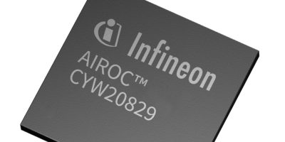
Infineon includes Bluetooth 5.5 in Airoc SoCs

The newly release Bluetooth 5.4 specification is integrated in Infineon’s Airoc CYW20829 Bluetooth LE SoC. According to Infineon, with the right combination of low power and high performance, Airoc CYW20829 is designed to support the entire spectrum of Bluetooth Low Energy (LE) use cases including smart home, sensors, medical healthcare, lighting, Bluetooth Mesh networks, remote controls, human interface devices (mouse, keyboard, VR and gaming controllers), industrial automation and automotive designs.

CYW20829 is a dual-core Arm M33 device where one M33 core is reserved as the Bluetooth controller, and the second Arm Cortex-M33 is available for customer applications. The CPU subsystem provides 256k RAM, XIP interface for external flash, and a rich set of peripherals including CAN. Built-in security features include secure boot, secure execution environment, a TRNG, eFuse for custom keys and cryptography acceleration.

The recently released Bluetooth Core Specification 5.4 adds several significant capabilities to the existing specification, including PAwR (periodic advertising with response), encrypted advertisement data (EAD) and Le GATT security levels characteristic. PAwR enables energy-efficient, bi-directional communication in a large scale one-to-many or star topology. EAD provides a standardised approach to the secure broadcasting of data in advertising packets, advised Infineon.

With PAwR, thousands of Bluetooth 5.4-enabled electronic shelf labels (ESL) and sensors will have bidirectional communication with a single access point. Messages can contain commands, sensor data values or other data, as defined by the application layer. EAD enables the encrypted data over-the-star network to be authenticated and decrypted only by devices that have shared the session key previously. Additionally, LeGATT security levels characteristic enables devices to identify the security mode and level for GATT functionality. The combination of these features enable low power, efficient radio usage and secure star networks that can be deployed in large scale ESL and sensor applications.

“With Infineon’s AIROC CYW20829 Bluetooth LE SoC, our customers can achieve great RF performance, the latest Bluetooth features, built-in security, rich set of peripherals, and low power, all in one device,” said Shantanu Bhalerao, Vice President of the Bluetooth product line at Infineon. 

Airoc CYW20829 has best-in-class RF link budget, claimed Infineon, with an integrated power amplifier providing 10dBm of transmit output power and receive sensitivity of -98dBm for LE 1Mbits per second and -106dBm for LE Long Range 125kbits per second. 

The Airoc CYW20829 is supported by the ModusToolbox development environment which enables developers to accelerate time-to-market for Bluetooth-enabled IoT solutions.

The SoC is currently sampling to select customers.

http://www.infineon.com

> Read More

Renesas adds two Arm Cortex-M33 core MCUs to 32-bit RA family

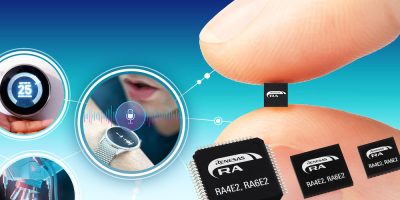
The RA4E2 and RA6E2 MCUs deliver up to 200MHz in compact packages and offer rich peripheral options for sensing, gaming, wearables and appliances, said Renesas.

They are both based on the Arm Cortex-M33 core with Arm TrustZone technology. The 100MHz RA4E2 Group and 200MHz RA6E2 Group of MCUs are optimised to provide power efficiency, said Renesas. They are available in 128kbyte and 256kbyte flash options and 40kbytes of SRAM. Connectivity options are on-chip CAN FD, USB, QSPI, SSI and I3C interfaces. The MCUs offer an upgrade path to other members of the RA family. 

The RA4E2 and the RA6E2 offer a cost-effective option with integrated CAN FD and space saving packages as small as a 4.0 x 4.0mm 36-pin BGA or a 5.0 x 5.0mm 32-pin QFN. 

All RA devices are supported by the Renesas flexible software package (FSP) that includes efficient drivers and middleware to ease the implementation of communications and improve functionality of peripherals. The FSP’s GUI simplifies and accelerates the development process, said Renesas. It enables flexible use of legacy code as well as compatibility and scalability with other RA family devices. Designers using FSP also have access to the full Arm ecosystem as well as Renesas’ extensive partner network, offering a wide range of tools that help speed time-to-market.

The RA4E2 Group includes five different options, spanning from 32-pin to 64-pin packages as small as 4.0 x 4.0mm, and 128kbyte of flash memory along with 40kbyte of SRAM. The devices use just 82 microA / MHz while executing from flash at 100MHz. They have an extended operating temperature range of -40 to +105 degrees C. 

The devices in the RA4E2 Group are based on a 100MHz Arm Cortex-M33 CPU core and can reduce system costs by virtue of the internal oscillator, general purpose I/O, advanced analogue, low voltage detection and internal reset function

The RA6E2 Group MCUs deliver 200MHz performance. Based on a 200MHz Arm Cortex-M33 CPU core, they also have low power operation ( 80 microA / MHz in active mode at 200MHz). The group includes 10 different parts, spanning from 32-pin to 64-pin packages as small as 4.0 x 4.0mm, and from 128kB to 256kbyte of flash memory along with 40kbyte of SRAM. Integrated communications options including USB 2.0 full-speed device, SCI, SPI, I3C, HDMI CEC, SSI, QSPI, and CAN FD and an integrated timer.

Renesas has designed a full Add-on Voice User Interface (VUI) using the RA6E2 MCU and other compatible devices from the Renesas portfolio. It can be added to devices such as smart thermostats or appliances. 

All RA4E2 and RA6E2 MCUs are available today with separate evaluation kits and fast prototyping boards available for both MCU groups.

http://www.renesas.com

> Read More

About Smart Cities

This news story is brought to you by smartcitieselectronics.com, the specialist site dedicated to delivering information about what’s new in the Smart City Electronics industry, with daily news updates, new products and industry news. To stay up-to-date, register to receive our weekly newsletters and keep yourself informed on the latest technology news and new products from around the globe. Simply click this link to register here: Smart Cities Registration