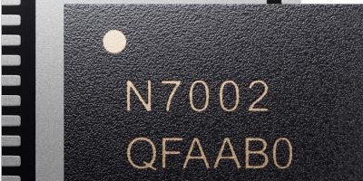
Rutronik offers Wi-Fi 6 seamless connectivity with Nordic’s nRF7002 

Nordic Semiconductor’s nRF7002 is a companion IC for integrating seamless Wi-Fi 6 connectivity into a range of applications. It is a cost-effective and power-saving option, said Rutronik, with high speed, improved range and the reliability of the latest Wi-Fi standard. 

The IC operates on both the 2.4 GHz and 5.0GHz Wi-Fi bands, offering a range of options for connecting to networks. The nRF7002 equips products with the latest Wi-Fi 6 technologies, making it suitable for use in medical or inventory tracking applications. Its low power consumption makes it particularly interesting for use in battery-powered wireless products, added Rutronik. 

The nRF7002 is designed to be used in conjunction with the nRF Connect software development kit (SDK). The platform has a number of tools and libraries for developing applications for which the nRF7002 is the optimal choice.

The nRF7002 complies with 802.11a/b/g/n/ac/ax- and has a 20MHz channel bandwidth with 64 QAM (MCS7) and 86Mbits per second PHY throughput.

The companion IC is currently unique in this form in the Nordic portfolio and can be combined with the company’s ultra low power technologies. It is also compatible with Nordic’s existing nRF52 and nRF53 series Bluetooth SoCs and nRF91 series cellular IoT systems in package (SiPs). As a result, Nordic’s Wi-Fi 6 companion IC nRF7002 is suitable for a wide range of applications, for example in smart cities, smart agriculture, smart home, wearables and medical devices. 

The nRF7002 from Nordic Semiconductor is available from the distributor, Rutronik.

Rutronik Elektronische Bauelemente was founded in 1973 and is an independent family-owned company based in Ispringen, Germany. It claims to be one of the world’s leading broadline distributors. It has more than 80 offices worldwide and logistics centres in Austin (Texas), Shanghai, Singapore, and Hong Kong to offer comprehensive customer support in Europe, Asia, and North America.

The company focuses on advanced materials, advanced measurement, processing and analytics, advanced robotics, automation, biotechnology, energy and power, future mobility, IIoT and internet of everything, industry 4.0, medical and healthcare, and transportation, logistics and supply chain. 

The company also offers customised logistics systems, reliable supply chain management, and logistics centres worldwide to ensure on-time delivery. The Rutronik24 e-commerce platform completes Rutronik’s range of services. 

http://www.rutronik.com

> Read More

Nordic Semiconductor disrupts IoT with low power wireless SoCs

A fourth generation, low power wireless SoC has been introduced by Nordic Semiconductor. The first SoC in the nRF54 series is the nRF54H20 and suitable for disruptive IoT applications demanding high processing power, excellent energy efficiency and security, said Nordic Semiconductor.

The nRF54 series of Bluetooth Low Energy (Bluetooth LE) SoCs add to Nordic’s portfolio of the nRF51, nRF52, and nRF53 series. At the same time it introduces a new hardware architecture fabricated on the GlobalFoundries 22FDX process node. 

Capable of supporting Bluetooth 5.4 and future Bluetooth specifications, plus LE Audio, Bluetooth mesh and Thread, Matter, the nRF54H20 will be the foundation for a new wave of revolutionary IoT end products, promised Nordic Semiconductor. Its combination of advanced features will enable complex end products that have previously been unfeasible, claimed the company.

The nRF54H20 comprises multiple Arm Cortex-M33 processors and multiple RISC-V coprocessors. The processors are clocked at up to 320MHz and each processor is optimised for a specific type of workload.  

The dedicated application processor features double the processing power (2x CoreMark) of the application processor in the nRF5340 SoC. The nRF54H20’s computing resources are supported by integrated memory comprising 2Mbyte non-volatile memory and 1Mbyte of RAM. The SoC’s level of integration will enable developers to shrink designs by replacing multiple components, such as application microcontroller, external memory and wireless SoC, with a single, compact device. In addition to advanced wearables, smart home, medical and LE Audio applications, the nRF54H20 SoC can be used for applications demanding complex machine learning (ML) and support for sensor fusion at the edge.

The nRF54H20 features several new digital and analogue interfaces, including a high performance external memory interface (400Mbytes per second), high speed USB (480bits per second), two I3C peripherals, a CAN FD controller and a 14-bit ADC. These interfaces are in addition to analogue and digital interfaces integrated on the nRF54H20.

The multi-protocol 2.4GHz radio ensures the nRF54H20 SoC is the first in the world to offer -100dBm RX sensitivity when receiving a 1Mbit per second Bluetooth LE signal, according to Nordic Semiconductor. Combined with up to 10dBm TX power, the nRF54H20 offers an ample link budget for enhanced robustness and longer range. The radio RX current consumption is just half that of the nRF5340, said Nordic. For applications that are mainly receivers, such as earbuds and wearables, the low energy consumption allows for more compact batteries or extended battery life, explained Nordic Semiconductor.

The nRF54H20 is a secure low power, multi-protocol SoC and is designed for PSA Certified Level 3, the highest level in the Platform Security Architecture (PSA) Certified IoT security standard. The SoC supports security services such as secure boot, secure firmware update and secure storage. It has cryptographic accelerators that are hardened against side-channel attacks and tamper sensors that detect an attack in progress and take appropriate action.

The nRF54H20 SoC is available for sampling now to selected customers.

http://www.nordicsemic.com

> Read More

Energy harvesting PMIC contributes to low power IoT

Adding to its range of power ICs, Nexperia has introduced the NEH2000BY power management IC (PMIC) for low power embedded applications, including the IoT.

The NEH2000BY PMIC recharges a battery or storage capacitor using energy harvested from ambient sources, such as light (which can be harvested using a photovoltaic cell). The PMIC will enable the development of electronic devices that are self-powered, smaller, and environmentally friendly, said Nexperia and exploit energy harvesting to help mitigate the environmental impact of the billions of batteries produced and discarded each year.

The PMIC makes it much easier to design energy harvesting solutions which can be up to 20x smaller than other competing offerings and do not require manual optimization for individual applications, claimed the company. It is designed without inductors, which simplifies PCB design and “significantly” reduces BoM and board size. The assembly area is just 12mm².

To achieve the highest conversion efficiency, energy harvesting must be able to adapt as the ambient energy source fluctuates. To this end, the NEH2000BY performs maximum power point tracking (MPPT), an adaptive algorithm to optimise how it transfers harvested energy, achieving optimum average conversion efficiency by up to 80 per cent. The MPPT algorithm combines speed with accuracy, allows the PMIC to adapt to environmental changes in less than one second: significantly faster than any other currently available solution, said Nexperia. By maximising the amount of energy harvested over the course of a day, the PMIC can broaden the number of applicable use cases, while the self-optimisation functionality and the ability to operate autonomously without pre-programming make it simpler to design products using ambient energy.

Nexperia’s energy harvesting technology enables economical energy harvesting from various ambient sources in applications consuming up to several mW of power, including wireless IoT nodes, wearable smart tags and electronic shelf labels.

Dan Jensen, general manager business group analogue and logic ICs at Nexperia commented: “The NEH2000BY . . . will allow the adoption of energy harvesting in a larger range of use cases. By eliminating the requirement to change batteries in these applications, NEH2000BY will significantly reduce the amount of hazardous waste produced, with enormous environmental benefits.”

The NEH2000BY is available in a 16-lead, 3.0 x 3.0mm QFN package and operates between -40 and +85 degrees C.

http://www.nexperia.com

> Read More

Infineon makes Secora Pay available in 28nm

Payment cards will have the capability to be offered in new, innovative designs, said Infineon, as it introduces its Secora Pay card payment technology is available on 28nm chip technology.

The Secora Pay platform allows manufacturers to efficiently produce robust dual interface cards for payment and multi-application use cases, explained Infineon Technologies.

The introduction of 28nm chip technology is believed to be the first 28nm technology card payment technology with embedded non-volatile memory. It is intended to side step the semiconductor shortages experienced in mature technology nodes.

The product family uses a security controller with certified software integrated into coil on module (CoM) chip modules. The devices use standardised inlays for easy and fast card production which are compatible with Secora Pay products on 65nm, 40nm and 28nm technology. One inlay sheet fits the existing and new Secora Pay products. 

The CoM system offers maximum flexibility in card design, said Infineon. It uses inductive coupling technology with copper wired card antennas. It is therefore perfectly suited for future market trends such as environmentally friendly cards made of recycled and ocean-bound plastic or wood, as well as high-performance dual-interface metal or LED cards.

Secora Pay products support the highest throughput in card production with minimal resources for manufacturing highly robust dual-interface cards, said Infineon. New services based on Secora Pay’s NFC tag enable further use cases such as initial card activation as well as authentication for online banking and for loyalty programmes.

“In recent years, touchless payment experience with dual-interface payment cards has become a global standard, among others also driven by the Covid-19 pandemic,” said Tolgahan Yildiz, head of payment solutions at Infineon’s connected secure systems division.

The Secora Pay portfolio us engineered to enable manufacturing and issuance of high quality dual-interface payment cards for high transaction performance with reliable security for trusted seamless payments, he added.

The global dual-interface payment card market is expected to grow at a compound annual growth rate of six percent from 2022 to 2027, starting from an estimated 2.6 billion units in 2022.

The 28nm technology products offer a simple onboarding process or migration path for card manufacturers, claimed Infineon. They are backwards-compatible with existing Secora Pay products in terms of card production, antenna design, personalisation and product certification for contactless and personalised performance, enabling contactless transactions within 155 milliseconds.

Product versions supporting the latest Visa and Mastercard applications are available now with extremely long approval life time. Certified applets for American Express, Discover and others will follow later this year, confirmed Infineon.

http://www.infineon.com

> Read More

About Smart Cities

This news story is brought to you by smartcitieselectronics.com, the specialist site dedicated to delivering information about what’s new in the Smart City Electronics industry, with daily news updates, new products and industry news. To stay up-to-date, register to receive our weekly newsletters and keep yourself informed on the latest technology news and new products from around the globe. Simply click this link to register here: Smart Cities Registration