NFC tag allows seamless mobile connectivity

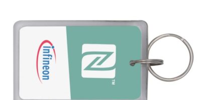
Infineon Technologies claims to have introduced the world’s first certified NFC Type 4B tag. It is claimed to be the first product worldwide certified by the NFC Forum that supports the contactless Type B protocol.

Near field communication (NFC) allows wireless communication between two electronic devices within a distance of approximately 4 cm. NFC tags use this technology to exchange data and to enable contactless payments using smart cards or mobile handsets. NFC tags provide smartphones with reliable data exchange and reference tags for interoperability testing with all types of internationally standardised NFC protocols. This latest NFC reference tag is based on SECORA Pay security, which has been approved under the NFC Forum Certification Program. This confirms their compliance with the Type 4A Tag and the Type 4B Tag.

NFC tags have been generally limited to use cases where security is not deemed to be critical – such as sharing URLs or exchanging business cards. However, they can also be combined with security critical payment applications. Users can activate services via NFC connectivity without having to open an app, and thus instantly connect their mobile handset to, for example, smart devices like wearables or access shared services such as pavement scooters with intuitive connectivity for everyday digital transactions.

The NFC reference tags are based on Infineon’s SPA1.1 module and are pre-loaded with NFC data exchange format (NDEF) files so developers can test a wide variety of smartphones for compliance with ISO/IEC 14443 Type A and Type B.

The Type A and Type B NFC tags are available in pairs.

http://www.infineon.com

> Read More

Renesas announces memory technology for AI

Renesas Electronics has developed an AI accelerator that performs convolutional neural network (CNN) processing at high speeds and low power.  A test chip with this accelerator has achieved the power efficiency of 8.8Tera operations per second per W (TOPS/W), which is the industry’s highest class of power efficiency, reports Renesas. The accelerator is based on the processing-in-memory (PIM) architecture, in which multiply-and-accumulate (MAC) operations are performed in the memory circuit as data is read out from that memory.

To create the new AI accelerator, Renesas developed three technologies. The first is a ternary-valued (-1, 0, 1) SRAM structure PIM technology that can perform large-scale CNN computations. The second is an SRAM circuit to be applied with comparators that can read out memory data at low power. The third is a technology that prevents calculation errors due to process variations in the manufacturing. Together, these technologies achieve a reduction in the memory access time in deep learning processing and a reduction in the power required for the MAC operations. As a result, the accelerator achieves the industry’s highest class of power efficiency while maintaining an accuracy ratio more than 99 per cent when evaluated in a handwritten character recognition test (MNIST), claims Renesas.

Before this development, the PIM architecture was unable to achieve an adequate accuracy level for large-scale CNN computations with single-bit calculations because the binary (0,1) SRAM structure was only able to handle data with values 0 or 1. Additionally, process variations in the manufacturing reduced the reliability of these calculations. The technologies developed by Renesas resolve these issues and can be applied to implement AI chips of the future and e-AI solutions for applications such as wearable equipment and robots that require both performance and power efficiency, says Renesas.

Since introducing the embedded AI (e-AI) concept in 2015, Renesas has defined classes based on the effectiveness of e-AI and applications that are implemented and has been developing e-AI solutions based on four classes: judging the correctness or abnormality of signal waveform data; judging correctness or abnormality using real-time image processing; performing recognition in real time and enabling incremental learning at an endpoint.

https://www.renesas.com 

> Read More

Arm introduces CPU and GPU for 5G mobiles

At Computex in Taiwan this week, Arm has unveiled the latest Cortex CPU, a new Mali GPU. Based on a new architecture and a processor for machine learning.

The latest Cortex CPU, the Cortex-A77 improves instruction per cycle (IPC) performance by 20 per cent, compared with the Cortex-A76 for machine learning, augmented reality and virtual reality (ML, AR and VR).

The Arm Mali-G77 GPU is based on Valhall architecture and is intended for use in mobile devices to deliver graphics at increased efficiency, according to Arm. Microarchitecture enhancements including engine, texture pipes, and load store caches, which achieve 30 per cent better energy efficiency and 30 per cent more performance density. The Valhall architecture is claimed to deliver close to 40 per cent performance improvement compared with the Mali-G76 in devices today.

Arm also says that it boosts inference and neural net (NN) performance for ML and to deliver more immersive games for mobile apps.

A dedicated ML processor delivers up to five tera operations per second (TOPS) per W as part of Project Trillium. The ML processor and open-source Arm NN software framework was announced in 2018 and enhancements to the ML processor include more than double energy efficiency to 5TOPS/W, memory compression improved by up to a factor or three and scaling to peak next-generation performance up to eight cores for up to 32TOPS.

http://www.arm.com

> Read More

Software development kit streamlines SLAM in mobile devices

To develop simultaneous localisation and mapping (SLAM) –enabled mobile devices, augmented reality/virtual reality (AR/VR) headsets, robots, autonomous vehicles and drones, Ceva offers the SLAM software development kit for CEVA-XM intelligent vision DSPs and NeuPro AI processors

The kit incorporates hardware, software and interfaces that can “significantly lower the entry barrier” to integrate efficient SLAM implementations into low-power embedded systems, says Ceva.

According to Ilan Yona, vice president and general manager of the vision business unit at Ceva: “SLAM is the underlying technology that enables high-accuracy 3D mapping of a device’s surroundings”. He believes that the company’s expertise in designing vision DSPs and software algorithms will introduced customers to 3D machine vision design.

The Ceva-SLAM software development kit has a detailed interface from a CPU to offload the heavy lifting SLAM blocks to the Ceva-XM DSP. These building blocks use the DSP to support both fixed point and floating point math and extend the device’s battery life. They also include capabilities for image processing (including feature detection, feature descriptors, feature matching), linear algebra (including matrix manipulation, linear equation solving) and fast sparse equation solving for bundle adjustment. The software development kit can run a full SLAM tracking module on the Ceva-XM6 DSP at 60 frames per second consuming just 86mW (using a frame size of 1280 x 720, running on Ceva-XM6 using TSMC’s 16nm process).

The software development kit, deployed with a Ceva-XM DSP or a NeuPro AI processor, can be used for visual positioning, classical and neural network workloads for imaging and vision using SLAM.

The Ceva-SLAM software development kit is available for licensing now, exclusively in conjunction with the Ceva-XM intelligent vision DSPs and NeuPro AI processors.

Ceva will presenting the Ceva-SLAM software development kit at the Embedded Vision Summit in Santa Clara, California, USA (Wednesday 22 May).

Ceva licenses signal processing platforms and artificial intelligence processors.  It provides low power IP for vision, audio, communications and connectivity including   DSP-based platforms for LTE/LTE-A/5G baseband processing in handsets, infrastructure and cellular IoT (NB-IoT and Cat-M) enabled devices, imaging and computer vision for any camera-enabled device, audio/voice/speech and low power always-on/sensing applications for IoT markets.

http://www.ceva-dsp.com

> Read More

About Smart Cities

This news story is brought to you by smartcitieselectronics.com, the specialist site dedicated to delivering information about what’s new in the Smart City Electronics industry, with daily news updates, new products and industry news. To stay up-to-date, register to receive our weekly newsletters and keep yourself informed on the latest technology news and new products from around the globe. Simply click this link to register here: Smart Cities Registration