Sensor hub DSP architecture makes sense of surroundings

Claimed to be the industry’s first high performance sensor hub DSP architecture, SensPro is configurable for parallel processing floating point and integer data types, as well as deep learning training and inferencing.

Ceva has designed it to handle the sensor processing and sensor fusion workloads for contextually-aware devices.

It addresses the need for specialised processors to efficiently handle the proliferation of different types of sensors that are required in smartphones, robotics, automotive, AR/VR headsets, voice assistants, smart home devices and for industrial and medical applications. These camera, radar, lidar, time of flight (ToF) sensors, microphones and inertial measurement units (IMUs) generate data types and bit-rates derived from imaging, sound, RF and motion, which can be used to create a full 3D contextually-aware device, says CEVA.

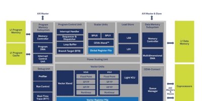
The SensPro architecture is built from the ground up to maximise performance per Watt for multi-sensor processing use cases. It combines high performance single and half precision floating-point maths required for high dynamic range signal processing, point cloud creation and deep neural network (DNN) training. It also has 8-bit and 16-bit parallel processing capacity for voice, imaging, DNN inference processing and simultaneous localisation and mapping (SLAM). SensPro incorporates the Ceva-BX scalar DSP, which offers a seamless migration path from single sensory system designs to multi-sensor, contextual-aware designs.

Dimitrios Damianos, technology and market analyst of the sensing division at Yole Développement (Yole) commented: “The proliferation of sensors in intelligent systems continues to increase, providing more precise modelling of the environment and context. Sensors are becoming smarter, and the goal is not to get more and more data from them, but higher quality of data especially in cases of environment/surround perception. . . .  where many sensors . . . must work together to make sense of their surroundings”.

Yohann Tschudi, technology & market analyst, computing and software, at Yole continued: “The challenge is to process and fuse different types of data from different types of sensors. Using a mix of scalar and vector processing, floating and fixed point math coupled with an advanced micro-architecture, SensPro offers system and SoC designers a unified processor architecture to address the needs of any contextually-aware multi-sensor device.”

SensPro uses a configurable eight-way VLIW architecture, allowing it to be easily tuned to address a range of applications. Its micro-architecture combines scalar and vector processing units and incorporates an advanced, deep pipeline enabling operating speeds of 1.6GHz at a 7nm process node.

A Ceva-BX2 scalar processor for control code execution has a 4.3 CoreMark/MHz score. It adopts a wide SIMD scalable processor architecture for parallel processing and is configurable for up to 1024 8×8 MACs, 256 16×16 MACs, dedicated 8×2 binary neural networks support, as well as 64 single precision and 128 half precision floating point MACs. This allows it to deliver 3TOPS for 8×8 networks inferencing, 20TOPS for binary neural networks inferencing, and 400GFLOPS for floating point arithmetic. Additionally, a memory architecture provides a bandwidth of 400Gbyte per second, four-way instruction cache, two-way vector data cache, DMA, and queue and buffer managers for offloading the DSP from data transactions.

Ceva also offers software and development tools, including an LLVM C/C++ compiler, Eclipse based integrated development environment (IDE), OpenVX API, software libraries for OpenCL, Ceva deep neural network (CDNN) graph compiler including the CDNN-Invite API for inclusion of custom AI engines, Ceva-CV imaging functions, Ceva-SLAM software development kit and vision libraries, ClearVox noise reduction, WhisPro speech recognition, MotionEngine sensor fusion, and the SenslinQ software framework.

Initially, SensPro DSPs will be available in three configurations:  SP250 (single vector unit with 256 8×8 MACs targeting imaging, vision, and sound centric applications), SP500F (single vector unit with 512 8×8 MACs and 64 single precision floating point MACs targeting SLAM applications) and SP1000 (dual vector units with 1024 8×8 MACs and binary networks support targeting AI applications).

The SensPro architecture and cores will be made available for general licensing from Q3 2020.

https://www.ceva-dsp.com

> Read More

Evaluation kit supports energy harvesting embedded controller

For the development of battery maintenance-free IoT equipment, Renesas Electronics has introduced the RE family, which encompasses the company’s current and future line-up of energy harvesting embedded controllers. The RE Family is based on Renesas’ proprietary Silicon on Thin Buried Oxide (SOTB) process technology. SOTB is claimed to dramatically reduce power consumption in both active and standby states, eliminating the need for battery replacement or recharging.

Following the introduction of the RE01 microcontrollers, the first of the RE family, the RE01 Group evaluation kit is now available to allow users working with the RE01

Hiroto Nitta, senior vice president, Head of SoC Business, IoT and Infrastructure Business Unit at Renesas, said: “We hope this will accelerate the spread of IoT equipment powered by energy harvesting.”

The RE01 evaluation kit includes an evaluation board with an RE01 embedded controller, an interface for the energy harvesting device and a rechargeable battery interface. There is also an Arduino-compatible interface for easy expansion and evaluation of sensor boards and a Pmod connector to expand and evaluate wireless functionality. There is also a low power memory in pixel (MIP) LCD expansion board so that users can evaluate display functions faster. The kit also contains sample code and application notes that  serve as references for power management design that eliminates the need for battery maintenance, and driver software that supports CMSIS, Arm’s Cortex Microcontroller Software Interface Standard. Sample code for low power ADCs, digital filter and fast Fourier transform (FFT) routines, 2D graphics MIP LCD displays, and secure boot and secure firmware update functions for improved security are available.

The kit can be used to adopt energy harvesting based on RE01 Group devices at the system level and will accelerate the development of equipment that does not require battery maintenance.

IAR Embedded Workbench for Arm which can use the high efficiency IAR C/C++ compiler, and e2 studio (note 2) which can use the free GNU compiler are available as the developmental environment.

The RE01 evaluation kit is available now.

http://www.renesas.com

> Read More

Microchip simplifies hardware-based IoT security

A pre-provisioned solution that provides secure key storage for low-, mid- and high-volume device deployments using the ATECC608A secure element is now available from Microchip Technology. According to the company, the Trust Platform for its CryptoAuthentication family enables companies of all sizes to implement secure authentication.

The platform consists of a three-tier offering, providing out-of-the-box pre-provisioned, pre-configured or fully customisable secure elements, allowing developers to choose the platform best suited for their individual design. As the first solution to provide ready-to-go secure authentication for the mass market, the first tier – Trust&GO – provides zero-touch pre-provisioned secure elements with a minimum orderable quantity (MOQ) as low as 10 units.

Device credentials are pre-programmed, shipped and locked inside the ATECC608A for automated cloud or LoRaWAN authentication onboarding. In parallel, corresponding certificates and public keys are delivered in a “manifest” file, which is downloadable via Microchip’s purchasing e-commerce store and select distribution partners.

With the ability to authenticate to any public or private cloud infrastructure, Microchip’s Trust Platform is also flexible and customisable. For customers who want more customisation, the program includes the TrustFlex and TrustCustom platforms.

The solution helps simplify provisioning logistics, says the company, making it easy for mass market customers to secure and manage edge devices without the overhead cost of third-party provisioning services or certificate authorities.

The second tier in the program, TrustFlex, offers the flexibility to use the customer’s certificate authority of choice while still benefiting from pre-configured use cases.

These use cases include baseline security measures such as transport layer security (TLS) hardened authentication for connecting to any IP-based network using any certificate chain, LoRaWAN authentication, secure boot, Over-the-Air (OTA) updates, IP protection, user data protection and key rotation. This can reduce the time and complexity involved in customising the device without requiring customised part numbers.

For customers who would like to customise their designs entirely, the third tier in the program – TrustCustom – provides customer-specific configuration capabilities and custom credential provisioning.

https://www.microchip.com

> Read More

Research indicates Pohoiki Beach chip for neural-inspired algortithms

An eight million neuron system, comprised of 64 Phokiki Beach chips, the codename for Loihi chips, is now available to the research community. The neuromorphic system will allow researchers to experiment with Lohi, Intel’s brain-inspired research chip, which applies the principles found in biological brains to computer architectures. Loihi enables users to process information up to 1,000 times faster and 10,000 times more efficiently than CPUs for specialised applications like sparse coding, graph search and constraint-satisfaction problems.

The early results success has led Intel to make Pohoiki Beach available to over 60 ecosystem partners, who will use the system to solve complex, compute-intensive problems, explained Rich Uhlig, managing director of Intel Labs.

Availability means researchers can now efficiently scale up neural-inspired algorithms — such as sparse coding, simultaneous localisation and mapping (SLAM), and path planning — that can learn and adapt based on data inputs.

Intel Labs hopes to scale the architecture to 100 million neurons later this year.

As new complex computing workloads become the norm, there is a growing need for specialised architectures designed for specific applications. This will be achieved by continued process node scaling in the same vein as the power-performance increases achieved by Moore’s Law.

Using the Pohoiki Beach neuromorphic system rather than general purpose computing technologies, Intel hopes to realise gains in speed and efficiency in autonomous vehicles, smart homes and cybersecurity.

“With the Loihi chip we’ve been able to demonstrate 109 times lower power consumption running a real-time deep learning benchmark, compared to a [graphics processor unit] GPU, and five times lower power consumption compared to specialised IoT inference hardware,” said Chris Eliasmith, co-CEO of Applied Brain Research and professor at University of Waterloo. He continued: “As we scale the network up by 50 times, Loihi maintains real-time performance results and uses only 30 per cent more power, whereas the IoT hardware uses 500 per cent more power and is no longer real-time.”

In another research project, Loihi has been used in a neural network that imitates the brain’s underlying neural representations and behaviour. “The SLAM solution emerged as a property of the network’s structure,” explained Konstantinos Michmizos of Rutgers University. “We benchmarked the Loihi-run network and found it to be equally accurate while consuming 100 times less energy than a widely used CPU-run SLAM method for mobile robots,” he said.

Later this year, Intel will introduce an even larger Loihi system, named Pohoiki Springs. Intel’s engineers expect that measurements from these research systems will quantify the gains that are achievable with neuromorphic-computing methods and will clarify the application areas most suitable for the technology. This research paves the way for the eventual commercialisation of neuromorphic technology.

The Intel’s Nahuku boards pictured each contain eight to 32 Intel Loihi neuromorphic chips, interfaced to an Intel Arria 10 FPGA development kit.

(Credit: Tim Herman/Intel Corporation)

http://www.intel.com

> Read More

About Smart Cities

This news story is brought to you by smartcitieselectronics.com, the specialist site dedicated to delivering information about what’s new in the Smart City Electronics industry, with daily news updates, new products and industry news. To stay up-to-date, register to receive our weekly newsletters and keep yourself informed on the latest technology news and new products from around the globe. Simply click this link to register here: Smart Cities Registration