Passive balancing allows all cells to appear to have the same capacity

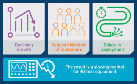
In the automotive and transportation marketplace, large battery stacks provide high output power without producing harmful emissions (that is, carbon monoxide and hydrocarbons) associated with gasoline-powered combustion engines. Ideally, each individual battery in the stack equally contributes to the system. However, when it comes to batteries, all batteries are not created equally. Even batteries of the same chemistry with the same physical size and shape can have different total capacities, different internal resistances, different self-discharge rates, etc. In addition, they can age differently, adding another variable in the battery life equation.

A battery stack is limited in performance by the lowest capacity cell in the stack; once the weakest cell is depleted, the entire stack is effectively depleted. The health of each individual battery cell in the stack is determined based on its state of charge (SoC) measurement, which measures the ratio of its remaining charge to its cell capacity. SoC uses battery measurements such as voltage, integrated charge and discharge currents, and temperature to determine the charge remaining in the battery. Precision single-chip and multichip battery management systems (BMS) combine battery monitoring (including SoC measurements) with passive or active cell balancing to improve battery stack performance. These measurements result in:

X Healthy battery state of charge independent of the cell capacity

X Minimised cell-to-cell state of charge mismatch

X Minimised effects of cell ageing (ageing results in lost capacity)

Passive and active cell balancing offer different advantages to the battery stack and Analog Devices offers solutions in our battery management product portfolio for both methods. Let’s first examine passive balancing.

Passive Balancing Allows All Cells to Appear to Have the Same Capacity

Initially, a battery stack may have fairly well matched cells. But over time, the cell matching degrades due to charge/discharge cycles, elevated temperature, and general ageing. A weak battery cell will charge and discharge faster than stronger or higher capacity cells and thus it becomes the limiting factor in the run-time of a system. Passive balancing allows the stack to look like every cell has the same capacity as the weakest cell. Using a relatively low current, it drains a small amount of energy from high SoC cells during the charging cycle so that all cells charge to their maximum SoC. This is accomplished by using a switch and bleed resistor in parallel with each battery cell.

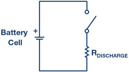
Figure 1. Passive cell balancer with bleed resistor.

The high SoC cell is bled off (power is dissipated in the resistor) so that charging can continue until all cells are fully charged.

Passive balancing allows all batteries to have the same SoC, but it does not improve the run-time of a battery-powered system. It provides a fairly low cost method for balancing the cells, but it wastes energy in the process due to the discharge resistor. Passive balancing can also correct for long-term mismatch in self discharge current from cell to cell.

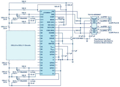
Figure 2. LTC6804 application circuit with external passive balancing.

Multicell Battery Monitors with Passive Balancing

Analog Devices has a family of multicell battery monitors that include passive cell balancing. These devices feature a stackable architecture, allowing hundreds of cells to be monitored. Each device measures up to 12 series of connected battery cells with a total measurement error of less than 1.2 mV. The 0 V to 5 V per cell measurement range makes them suitable for most battery chemistries. The LTC6804 is shown in Figure 2.

The LTC6804 features internal passive balancing (Figure 3) and can also be configured with external MOSFETs if desired (Figure 4). It also has an optional programmable passive balancing discharge timer that allows the user more system configuration flexibility.

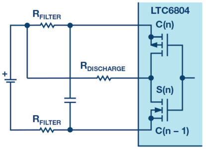
Figure 3. Passive balancing with internal discharge switch.

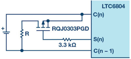
Figure 4. Passive balancing with external discharge switch.

For customers that wish to maximise system run-time and charge more efficiently, active balancing is the best option. With active cell balancing, energy is not wasted, but rather redistributed to other cells in the stack while both charging and discharging. When discharging, the weaker cells are replenished by the stronger cells, extending the time for a cell to reach its fully depleted state. For more on active balancing, see the technical article “Active Battery Cell Balancing.”

About the Authors

Sam Nork has worked for Analog Devices’ Power Products Business Unit (previously Linear Technology) since 1988. As a general manager and design director, Sam leads a development team of over 120 engineers focused on battery charger, ASSP, PMIC, and consumer power products. He has personally designed and released numerous portable power management integrated circuits, and is inventor/co-inventor on 11 issued patents. Prior to joining Linear Technology, Sam worked for Analog Devices in Wilmington, MA as a product/test development engineer. He received A.B. and B.E. degrees from Dartmouth College. He can be reached at sam.nork@analog.com.

Kevin Scott works as a product marketing manager for the Power Products Group at Analog Devices, where he manages boost, buck-boost, and isolated converters, as well as drivers and linear regulators. He previously worked as a senior strategic marketing engineer, creating technical training content, training sales engineers, and writing numerous website articles about the technical advantages of the company’s broad product offering. He has been in the semiconductor industry for 26 years in applications, business management, and marketing roles.

Kevin graduated from Stanford University in 1987 with a B.S. in electrical engineering and started his engineering career after a brief stint in the NFL. He can be reached at kevin.scott@analog.com.

> Read More

MEASURING THE IMPACT OF 5G

How Electronic Test and Measurement (ETM) Manufacturers Can Prepare for and Benefit from 5G

5G Is Coming

For many, that short statement is both a beacon of hope and a source of trepidation. This is especially true for test equipment manufacturers. While 5G offers the opportunity for healthy growth, there are several factors that will make reaping benefits from this generation of wireless broadband technology more challenging than it was for its predecessors.

Let’s start with the current situation for electronic test and measurement (ETM) manufacturers. What generates growth in the wireless ETM business is the combination of new handset models, an increasing volume of annual handset shipments, and wireless technology advancements that drive new infrastructure equipment. We have seen a reduction in the growth rate of handset shipments, as annual shipment volumes have started to exceed 1 billion units. At the same time, mergers and acquisitions in the wireless infrastructure industry have reduced the number of customers in that segment. Finally, ETM manufacturers have also been coping with delays in the deployment of LTE-advanced carrier aggregation in major markets. The result is a slowing market for LTE R&D and production test equipment, as the industry awaits the technology shift to 5G.

A slowing market for LTE test equipment has manufacturers eagerly awaiting the acceleration of 5G.

5G Is Coming—with Challenges

As wireless broadband technology has evolved from generation to generation—and especially from feature to feature—ETM manufacturers have often been able to rely on software upgrades to adapt to changes. The move to 5G, however, is seen as a giant stride forward that will require new and far more complex solutions.

Behind the faster speed, reduced latency, increased capacity, and improved reliability of 5G are new and less familiar technologies, such as millimeter wave, massive MIMO, and adaptive beamforming—all of which will demand significantly more advanced base stations and customer devices. The most substantial change to the 5G physical layer is the option for millimeter wave transmission coupled with adaptive beamforming requiring a large number of antenna elements. While millimeter wave transmission is a familiar technology for point-to-point, line-of-sight wireless backhaul, using those frequencies in a cellular topology, where each cell serves hundreds or thousands of mobile users, and where many antennas will be integrated into advanced device packaging, is challenging and uncharted territory. In order to research, develop, and test the new technologies behind 5G, ETM equipment will have to deliver far more advanced capabilities than previous generations of equipment. The ETM challenge is made more difficult by the fact that the 5G standards have not yet been finalized. And, like previous generations of wireless technology, there is the very strong desire by operators to be first with deployed networks, intensifying the need for ETM equipment early in the technology lifecycle.

Normally, this list of challenges would excite and energize an R&D group. However, the slackening growth in LTE ETM equipment has left some manufacturers with far fewer resources to devote to 5G innovation and development.

A Peek Behind the Curtain

If you want to go fast, go alone. If you want to go far, go together. While 5G introduces significant hurdles, they’re not insurmountable, especially if you subscribe to the wisdom of the African proverb above. New levels of cooperation can be seen throughout the wireless industry. Instrumentation, wireless infrastructure, semiconductor, and software organizations are working together with standards bodies, research organizations, and government regulators worldwide to ensure that 5G is a unified standard addressing the many challenging performance goals, including unprecedented speed, connection density, and ubiquity. Association with important wireless industry organizations such as ITU and 3GPP, and collaboration with any of the multitude of important research organizations, such as NIST and any of the numerous 5G research alliances, is a first step toward greater understanding of the 5G technology trajectory. In addition, ETM manufacturers appear to be gaining a better foothold in the 5G market by forming partnerships and alliances with suppliers.

Moving supplier relationships from highly transactional to being more collaborative can bring greater effectiveness to ETM manufacturers. Knowledge sharing and close collaboration with private companies, including operators and suppliers, is essential to timely delivery of new test products with features that are best aligned with early market needs. Nondisclosure agreements and other proprietary arrangements are giving manufacturers early access to new ideas and emerging technologies that are further enabling the technological breakthroughs required to deliver 5G test capabilities.

Component suppliers are providing information to optimize the performance of existing products beyond published data or are going a step further, such as creating part derivatives to meet specific needs. The right partnerships can bolster an ETM organization’s strengths with early access to advanced technology. Further, by transferring design work to experienced suppliers, an ETM manufacturer can free up scarce engineering resources—allowing them to focus on their strength of delivering value-added product features.

Combined, the partnering activities outlined above are helping ETM manufacturers get the solutions they need, accelerating their own schedules, and helping them and their customers succeed.

The Challenge to Develop Ahead of Standards

With the desire to reduce time to market and meet the demands of 5G, ETM manufacturers need to develop equipment prior to standards being finalized. Because 5G standards will remain in flux for the foreseeable future, working with the right supplier is giving manufacturers access to high performance solutions across the entire signal chain, from millimeter wave to bits. In that way, even as the 5G standard changes, there will be no need to scrap the original hardware design.

Integration

ETM manufacturers will face increased demands for greater capabilities and lower costs. As a result, test products for 5G will be far more complex than those of generations before. Looking beyond individual components to chipsets and system solutions is helping manufacturers squeeze more performance out of limited space and lower cost targets—something especially demanded of modular instrumentation. At the same time, this high level of integration, as well as the increased signal chain count required for MIMO and beamforming, is putting even greater demands on power. By working with suppliers, especially those with the broadest portfolio of products, it’s becoming possible to improve engineer components into complete signal chain solutions to meet the demanding performance, power, space, and time-to-market requirements of tomorrow’s instrumentation.

Ready or Not

5G is an evolutionary leap rather than a simple generational step up. While questions still remain about what 5G will be when it arrives, there is no doubt that it’s on the way. Whether 5G becomes an opportunity for ETM manufacturers will depend heavily on whether they are ready when this new technology arrives. Embracing partnerships and alliances with key suppliers will significantly help ETM manufacturers thrive in the coming 5G market.


By Randy Oltman, Systems Applications Manager, Analog Devices

> Read More

Vehicle Tracking Systems: Anytime, Anywhere, Anyhow

A vehicle tracking system is ideal for monitoring either a single car or an entire fleet of vehicles. A tracking system consists of automatic tracking hardware and software for data collection (and data transmission if required). The global fleet management market size was valued at USD $8 billion in 2015 and is anticipated to exceed USD $22 billion by 2022, growing at a CAGR of over 20% from 2016 to 2023 (Source: Global Market Insights). The rising demand for commercial vehicles in regions such as Latin America, the Middle East, and Africa also represents a potential growth opportunity. In more developed regions such as Europe and North America, integration of Internet of Things (IoT) technology in vehicles is expected to boost the adoption rate of vehicle tracking systems, although the high cost of integration has slowed this progress. Further, the Asia Pacific vehicle tracking market size is anticipated to witness significant growth over the forecasted period, with Japan, India, and China being the primary driving countries. These emerging markets have high potential, primarily due to their many commercial vehicles.

Active vs. Passive Trackers
Active and passive trackers collect data in the same way and are equally accurate. The main difference between the two types involves time. Active trackers are also called real-time trackers, because they transmit data via satellite or a cellular network, which instantly indicates where the vehicle is located. In this way, a computer screen can display this movement in real-time. This makes active tracking the best choice for businesses interested in improving the efficiency of their deliveries and monitoring their employees driving in the field. An active tracker also has geo-fence capabilities (think of this feature like a force field), providing an alert when the vehicle enters or exits a predetermined location (Source: RMT Corporation). These kinds of systems can also help prevent theft and help recover stolen vehicles. Of course, active GPS tracking devices are more expensive than passive ones and require a monthly service fee.

Passive trackers, on the other hand, are less costly, are smaller, and are easier to conceal. Their downside is that they have limited data storage. They store the information on the device instead of transmitting the data to a remote location. The tracker must be removed from the vehicle and plugged into a computer to view any of its information. These systems are good for people tracking their mileage for work purposes, or for businesses interested in reducing the misuse of their vehicles. Also, they are often chosen for monitoring the actions of people as well (think of detective work). Passive trackers are a good choice if immediate feedback is not required and there is a plan to regularly check the device’s data.

Both types of trackers are portable in nature and have a relatively small form factor. Therefore, battery power is required, as is backup capability to preserve data in case of power loss. Due to the higher automotive system voltages and currents required to charge the battery (typically a single-cell Li-ion cell), a switchmode charger is desirable for its higher charging efficiency when compared to a linear battery charging IC, as less heat in the form of power dissipation is generated. In general, embedded automotive applications have input voltages up to 30 V, with some even higher. In these GPS tracking systems, a charger with the typical 12 V to single-cell Li-ion battery (3.7 V typical) with added protection to much higher input voltages (in case of voltage transients from battery excursions), plus some sort of backup capability would be ideal.

Design Issues for Battery Charging ICs
Traditional linear topology battery chargers are often valued for their compact footprints, simplicity, and modest cost. However, drawbacks of traditional linear chargers have included limited input and battery voltage ranges, higher relative current consumption, excessive power dissipation (heat generation), limited charge termination algorithms, and lower relative efficiency. On the other hand, switchmode battery chargers are popular choices due to their topology, flexibility, multichemistry charging, their high charging efficiencies that minimise heat to enable fast charge times, and their wide operating voltage ranges. Of course, trade-offs always exist. Some downsides of switching chargers include relatively high cost, more complicated inductor-based designs, potential noise generation, and larger footprint solutions. Modern lead acid, wireless power, energy harvesting, solar charging, remote sensor, and embedded automotive applications are predominantly powered by switchmode chargers for the positive reasons stated previously.

Traditionally, a tracker’s backup power management system for batteries consisted of multiple ICs, a high voltage buck regulator, and a battery charger, plus all the discrete components; not exactly a compact solution. Hence, early tracking systems were not very compact in form factor. A typical application for a tracking system uses an automotive battery and a 1-cell Li-ion battery for storage and backup.

Why is it then that a more highly integrated power management solution is needed for tracking systems? Primarily, it is needed to reduce the size of the tracker itself; smaller is better in this market. Furthermore, there are requirements for safely charging the battery and protecting the IC against voltage transients, a need for system backup in case system power goes away or fails, and for powering the relatively lower rail voltages of the general packet radio service (GPRS) chipsets at ~4.45 V.

Power Backup Manager

An integrated power backup manager and charger solution, which solves the outlined objectives requires the following attributes:
. Synchronous buck topology for high efficiency
. Wide input voltage range to accommodate a variety of input power sources, plus protection against high voltage transients
. Proper battery charge voltage to support the GPRS chipset
. Simple and autonomous operation with onboard charge termination (no microcontroller needed)
. PowerPath control for seamless switchover between input power and backup power during a power fail event; it also needs to provide reverse blocking if a shorted input occurs
. Battery backup capability for system load power when the input is not present or fails
. Small and low profile solution footprints due to space constraints
. Advanced packaging for improved thermal performance and space efficiency

To address these specific needs, Analog Devices recently introduced the LTC4091—a complete, Li-ion battery backup management system for 3.45 V to 4.45 V supply rails that must be kept active during a long duration main power failure. The LTC4091 employs a 36 V monolithic buck converter with adaptive output control to provide power to the system load and enable high efficiency battery charging from the buck output. When external power is available, the device can provide up to 2.5 A of total output current and up to 1.5 A of charge current for a single-cell, 4.1 V or 4.2 V Li-Ion battery. If the primary input source fails and can no longer power the load, the LTC4091 provides up to 4 A to the system output load from the backup Li-ion battery via an internal diode, and relatively unlimited current if an external diode transistor is used. To protect sensitive downstream loads, the maximum output load voltage is 4.45 V. The device’s PowerPath control provides a seamless switchover between input power and backup power during a power fail event and enables reverse blocking with a shorted input. Typical applications for the LTC4091 include fleet and asset tracking, automotive GPS data loggers and telematics systems, security systems, communications, and industrial backup systems.

The LTC4091 includes 60 V absolute maximum input overvoltage protection, making the IC immune to high input voltage transients. The LTC4091’s battery charger provides two pin selectable charge voltages optimized for Li-ion battery backup applications: the standard 4.2 V and a 4.1 V option that trades off battery run time for increased charge/discharge cycle life. Other features include soft-start and frequency fold-back to control output current during startup and overload, as well as trickle charge, automatic recharge, low battery precharge, charge timer termination, thermal regulation, and a thermistor pin for temperature-qualified charging.

The LTC4091 is housed in a low profile (0.75 mm) 22-lead 3 mm × 6 mm DFN package with a backside metal pad for excellent thermal performance. The device operates from –40°C to +125°C. Figure 1 shows its typical application schematic.


Figure 1. LTC4091 typical application schematic.

Thermal Regulation Protection
To prevent thermal damage to the IC or surrounding components, an internal thermal feedback loop automatically decreases the programmed charge current if the die temperature rises to approximately 105°C. Thermal regulation protects the LTC4091 from excessive temperature due to high power operation or high ambient thermal conditions, and allows the user to push the limits of the power handling capability with a given circuit board design without risk of damaging the LTC4091 or external components. The benefit of the thermal regulation loop is that charge current can be set according to actual conditions, rather than worst-case conditions with the assurance that the battery charger will automatically reduce the current in worst-case conditions.
Automotive Cold-Crank Ride Through
Automotive applications experience large dips in supply voltage, such as during a cold-crank event, which can cause the high voltage switching regulator to lose regulation, resulting in excessive VC voltage and consequently excessive output overshoot when VIN recovers. To prevent overshoot when recovering from a cold-crank event it is necessary to reset the LTC4091’s soft-start circuit via the RUN/SS pin. Figure 2 below shows an example of a simple circuit that automatically detects a brown-out condition and resets the RUN/SS pin, re-engaging the soft-start feature and preventing damaging output overshoot.


Figure 2. Cold-crank ride-through circuit.

Conclusion
The adoption rates of automotive and fleet vehicle tracking systems are on the rise. Modern tracker form factors have shrunk and features have grown to include active data transmission for real-time tracking. Furthermore, backup capability and lower voltages to power the system GPRS chipset are needed. Analog Devices’ LTC4091 is a high voltage, high current buck battery charger and PowerPath backup manager with thermal regulation and other extensive protection that comprises a 1-chip, compact, powerful, and flexible solution for vehicle tracking applications, thus making a designer’s task simpler and easier.

Steve Knoth [steve.knoth@analog.com] is a senior product marketing engineer in Analog Devices’ Power by Linear™ Group. He is responsible for all power management integrated circuit (PMIC) products, low dropout regulators (LDOs), battery chargers, charge pumps, charge pump-based LED drivers, supercapacitor chargers, low voltage monolithic switching regulators, and ideal diode devices. Prior to joining Analog Devices (former Linear Technology) in 2004, Steve had held various marketing and product
engineering positions since 1990 at Micro Power Systems, Analog Devices, and Micrel Semiconductor. He earned his bachelor’s degree in electrical engineering in 1988 and a master’s degree in physics in 1995, both from San Jose State University. Steve also received an M.B.A. in technology management from the University of Phoenix in 2000. In addition to enjoying time with his kids, Steve can be found tinkering with pinball/arcade games or muscle cars; and buying, selling, and collecting vintage toys and movie/
sports/automotive memorabilia.

> Read More

2G to 5G Base Station Receiver Design Simplified by Innovative Integrated Transceivers

Base station receiver design can be a daunting task. Typical receiver components such as mixers, low noise amplifiers (LNAs), and analog-to-digital converters (ADCs) have progressively improved over time. However, architectures have only changed slightly. The limitation in architectural choices have held back base station designers from differentiating their products in the marketplace. Recent product developments, particularly integrated transceivers, have significantly relaxed some of the constraints of even the most challenging base station receiver designs. The new base station architecture offered by these transceivers allows base station designers more choices and ways to differentiate their product.

The family of integrated transceivers discussed in this article are the industry’s first to support all existing cellular standards, 2G to 5G, and cover the full sub-6 GHz tuning range. These transceivers allow base station designers to adopt a single, compact radio design across all band and power variants.

First, let’s review several base station classes. The well-known standards body 3GPP has several defined base station classes. These base station classes go by various names. In broad terms, the largest base stations, or wide area base stations (WA-BS), offer the most geographical coverage and number of users. They also output the highest power and must provide the best receiver sensitivity. Each progressively smaller base station requires less output power and a relaxed receiver sensitivity.

Table 1. Table 1. Various Base Station Sizes

In addition, 3GPP also defines different modulation schemes. Broadly speaking, a practical breakdown of modulation schemes is into non-GSM (including LTE and CDMA types of modulation) and GSM-based modulation—particularly multicarrier GSM (MC-GSM). Of the two broad schemes, GSM is the most demanding in terms of RF and analog performance. Also, as higher throughput radios have become more common, MC-GSM has become the norm over the single carrier GSM case. Generally, a radio front end in a base station that can support MC-GSM performance can also handle non-GSM performance. Carriers that handle MC-GSM will have more flexibility in market opportunities.

Historically, base stations have been composed of discrete components. We believe today’s integrated transceivers can replace many discrete components and offer system advantages as well. But first, we need to discuss the challenges of base station receiver design.

The wide area or macrobase station has traditionally been the most challenging and expensive receiver design, and historically has been the workhorse of our wireless communications networks. What makes it so challenging? In a word, sensitivity.

A base station receiver must achieve desired sensitivity under specific conditions. Sensitivity is a figure of merit of how well a base station receiver can demodulate a desired weak signal from handsets. Think of sensitivity as determining the farthest a base station can get from a handset while maintaining a connection. Sensitivity can be categorized in two ways: 1) static sensitivity without any external interference and 2) dynamic sensitivity with interference.

Let’s focus on static sensitivity, first. In engineering parlance, sensitivity is determined by the system noise figure (NF). A lower noise figure means better sensitivity. The desired sensitivity is achieved by increasing gain to achieve the desired system NF, and gain is generated by an expensive component called a low noise amplifier (LNA). The higher the gain, the more an LNA costs in dollars and power.

Unfortunately, there’s a trade-off with dynamic sensitivity. Dynamic sensitivity means that static sensitivity can get worse with interference. Interference is any unwanted signal that appears at the receiver, including signals from the outside world or signals generated unintentionally by the receiver, such as intermodulation products. Linearity in this context describes how well a system can handle interference.

In the presence of interference, our system loses the sensitivity we worked so hard to achieve. This trade-off gets worse with higher gain, because gain typically comes with lower linearity. In other words, too much gain degrades linearity performance, which leads to sensitivity degradation under strong interference.

Wireless communication networks are designed such that the burden of network performance is on the base station side as opposed to the handset side. WA-BSs are designed to cover a large area and achieve excellent sensitivity performance. A WA-BS must have the best static sensitivity to support handsets at the cell edge where the signal from handset is very weak. On the other hand, under interference or blocking conditions a WA-BS receiver’s dynamic sensitivity still needs to be good. The receiver still must exhibit good performance on a weak signal from a handset, even while a strong signal from a handset near the base station generates interference.

The following signal chain is a simplified typical discrete component-based system receiver. The LNA, mixer, and variable gain amplifier (VGA) are referred to as the RF front end. The RF front end is designed with a noise figure of 1.8 dB, while the ADC has a noise figure of 29 dB, and in the analysis in Figure 1, the RF front-end gain is swept on the x-axis to show the system sensitivity.

Figure 1. Typical discrete receiver signal chain, simplified.

Now let’s compare a simplified transceiver receive signal chain. One can see the transceiver receive signal chain bill of materials is smaller than the comparable discrete component signal chain. Additionally, the transceivers are designed with two transmitters and two receivers on chip. The apparently simple integration hides the elegance of the receiver design, which typically achieves a 12 dB noise figure. The following analysis shown in Figure 2 will show how the sensitivity pays off in a system.

Figure 2. Typical transceiver/receiver signal chain, simplified.

Figure 3 shows the RF front-end gain vs. static sensitivity for the above two implementations. A WA-BS works in the region where the sensitivity is almost to meet tightest sensitivity requirement. In contrast, a small cell works where the sensitivity curve slope is steepest, while still meeting the standard with a small margin. The transceiver achieves the desired sensitivity with much less RF front-end gain for both the WA-BS and small cell.

Figure 3. Discrete receiver vs. transceiver/receiver sensitivity.

What about dynamic sensitivity? In the RF front-end gain region, where we would design wide area base stations using a transceiver, dynamic sensitivity is also much better than a discrete solution. This is because lower gain RF front ends typically have higher linearity at a given power consumption. In discrete solutions, which typically use high gain, linearity is often dominated by the RF front end. In transceiver designs, degradation in sensitivity due to interference is dramatically reduced compared to a discrete solution.

It’s worth mentioning that in the presence of too much interference, systems are designed to reduce gain to a point where the interference can be tolerated and increase the gain when the interference is reduced. This is referred to as automatic gain control (AGC). Any reduction in gain is also going to reduce the sensitivity. If a system can tolerate the interferers, it is often best to keep the gain as high as possible to maximize sensitivity. AGC is a topic for a future discussion.

In summary, two outstanding features of this class of transceivers are excellent noise figure and higher immunity to interference. Using a transceiver in your signal chain means you can achieve a desired static sensitivity with much less front-end gain. In addition, the lower level of interference means you can achieve better dynamic sensitivity. If you need a LNA at all, it will be a less costly LNA and consume less power. You can also make different design trade-offs elsewhere in the system to take advantage of these features.

Today, there are configurable transceiver products in the market that fill a role in both wide area and small cell base station designs. Analog Devices is taking a leadership role in this new approach, with ADRV9009 and ADRV9008 products are
well-suited for wide area base stations and MC-GSM levels of performance. Additionally, the AD9371 family offers options with non-GSM (CDMA, LTE)  performance and bandwidth, but more power optimization.

This article is far from a thorough overview. The topic of sensitivity will receive a deeper treatment in our follow-up articles. Additionally, other challenges in base station receiver design include automatic gain control (AGC) algorithms, channel estimation, and equalization algorithms, etc. We plan to follow this article with a series of technical articles with the aim of simplifying your design process and improving your receiver system understanding.

About the Authors

Jon Lanford works as a system and firmware verification manager in the Transceiver Product Group at Analog Devices Greensboro. He has worked at ADI since completing his master’s degree in electrical engineering from North Carolina State University in 2003. His previous engineering roles include gigasample pipeline ADC design and calibration algorithm design, as well as test development for transceivers. He can be reached at jonathan.lanford@analog.com.

Kenny Man’s 25 year career has spanned across system design on high speed instrumentation and wireless base stations, system applications, and system architecture for wireless infrastructure in telecom equipment companies and semiconductor companies. His present role is in product engineering where he wants to better contribute to the building blocks of communication infrastructure. His hobbies include hiking, snow skiing, and reading history. He can be reached at kenny.man@analog.com.

> Read More

About Smart Cities

This news story is brought to you by smartcitieselectronics.com, the specialist site dedicated to delivering information about what’s new in the Smart City Electronics industry, with daily news updates, new products and industry news. To stay up-to-date, register to receive our weekly newsletters and keep yourself informed on the latest technology news and new products from around the globe. Simply click this link to register here: Smart Cities Registration