40V Input, 3.5A Silent Switcher µModule Regulator for Automotive and Industrial Applications

Low Noise Silent Switcher Architecture Simplifies EMI Design

Automotive, transportation, and industrial applications are noise sensitive and demand low EMI power solutions. Traditional approaches control EMI with slowed down switching edges or lower switching frequency. Both have undesired effects, such as reducing efficiency, increasing minimum on- and off-times, and requiring a large solution. Alternative solutions such as an EMI filter or metal shielding add significant costs in required board space, components, and assembly, while complicating thermal management and testing.

Our low noise μModule® technology offers a breakthrough in switching regulator design. The LTM8003 regulator within the µModule package uses a proprietary Silent Switcher® architecture to minimise EMI emissions while delivering high efficiency at high switching frequencies. The architecture of the regulator and the internal layout of the µModule device are designed so that the input loop of the regulator is minimised. This significantly reduces the switching node ringing and the associated energy stored in the hot loop, even with very fast switching edges. This quiet switching offers excellent EMI performance while minimising the ac switching losses, allowing the regulator to operate at high switching frequencies without significant efficiency loss.

This architecture, combined with spread spectrum frequency operation, greatly simplifies the EMI filter design and layout, which is ideal for noise sensitive environments. Figure 1 shows a simple EMI filter on the input side, enabling the demo circuit to pass the CISPR 25 Class 5 standard with plenty of margin, as shown in Figure 2.


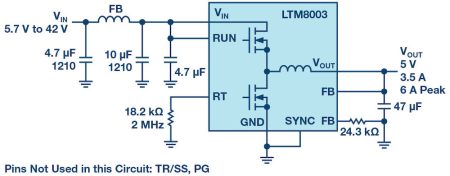
Figure 1. A 5V converter with a simple EMI filter at the input passes CISPR 25 Class 5.

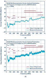
Figure 2. DC2416A demonstration circuit passes radiated EMI spectrum CISPR 25 Class 5.

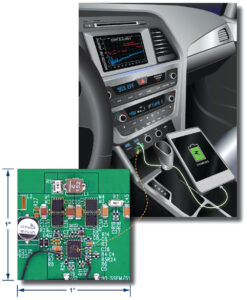
Continuous 3.5A with Peak Current Capability 6A

The internal regulator is capable of safely delivering up to 6A of peak output current, and no extra thermal management – airflow or heat sink – is required for the LTM8003 to continuously support a 3.5A load at 3.3V or 5V from a nominal 12V input. This meets the needs of the battery-powered applications in industrial robotics, factory automation, and automotive systems.

Wide Operation Temperature Range from –40°C to +150°C

Automotive, industrial, and military applications require power supply circuits to operate continuously and safely in ambient temperatures over 105°C or require significant headroom for a thermal rise. The LTM8003H is designed to meet specifications over a –40°C to +150°C internal operating temperature range. The internal over-temperature protection (OTP) monitors the junction temperature and stops switching when the junction temperature is too hot.

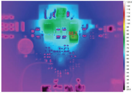
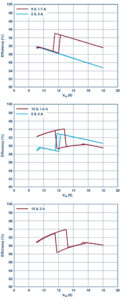
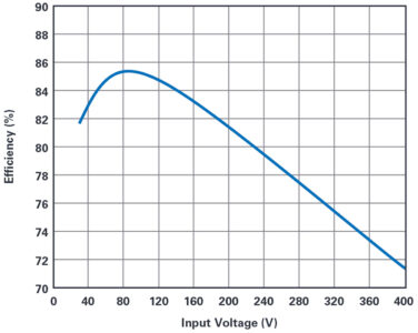
Figure 3a shows a 3.5A, 5V solution that operates from a wide-ranging 7V to 40V input. The thermal performance at a nominal 12V input is shown in Figure 3b. The typical efficiency is above 92% with a 12V input and 2A load.

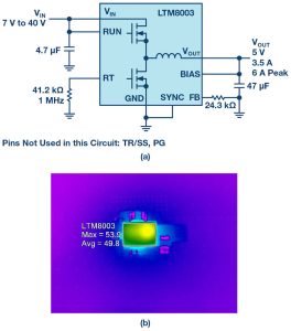
Figure 3. A 5V, 3.5A solution for 7V to 40V inputs using the H-grade version. Thermal imaging shows no need for bulky heat mitigation components.


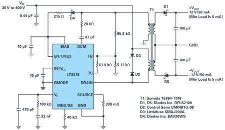
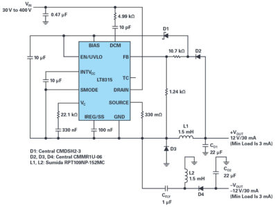
Negative Output –5V from +3.5V to +35V Input

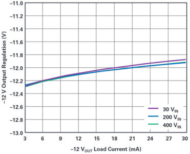
Figure 4 shows a solution for a –5V, 4A output from a nominal 12V input, with a maximum of 35V input. The BIAS pin should be connected to GND.

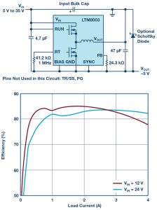
Figure 4. A –5V supply from a +5V to +35V input delivers current up to 4A.

Conclusion

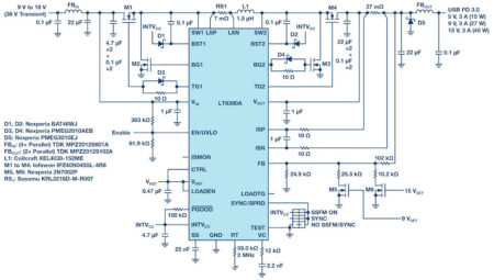
The LTM8003 is a wide input and output range, low noise, 3.5A step-down µModule regulator featuring the Silent Switcher architecture. Inputs from 3.4V to 40V can produce outputs from 0.97V to 18V, eliminating the need for intermediate regulation from batteries or industrial supplies. The pinout is specifically designed to be FMEA compliant, so the output stays at or below the regulation voltage during adjacent pin shorts, single-pin shorts to ground, or pins left floating. Redundant pins enhance electrical connections in the event a solder joint weakens or opens due to vibration, aging, or wide temperature variations, such as in automotive and transportation applications.

A complete solution fits a compact space not much larger than the 6.25mm × 9mm × 3.32mm, BGA footprint of the LTM8003, including the input and output capacitors. The quiescent current of typically 25µA and wide temperature operation from –40°C to +150°C (H-grade) make it ideal for circumstances where space is tight, the operational environment is harsh, and low quiescent current and high reliability are mandatory. Its features help minimise design effort and meet the stringent standards for industrial robotics, factory automation, avionics, and automotive systems.

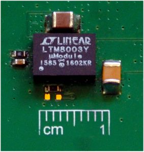
Figure 5. A complete step-down solution is barely larger than the 6.25mm × 9mm footprint of the LTM8003 µModule regulator.


About the Author

Zhongming Ye is a senior applications engineer for power products at Analog Devices, Inc., in Milpitas, California. He has been working at Linear Technology (now part of ADI) since 2009 to provide application support on various products including buck, boost, flyback, and forward converters. His interests in power management include high performance power converters and regulators of high efficiency, high power density, and low EMI for automotive, medical, and industrial applications. Prior to this, he worked at Intersil for three years on PWM controllers for isolated power products. He obtained a Ph.D. in electrical engineering from Queen’s University, Kingston, Canada. Zhongming was a senior member of IEEE Power Electronics Society. He can be reached at zhongming.ye@analog.com.

> Read More

Ensuring Data Integrity with the Internet of Things

Given the explosive growth in the number of things in the Internet of Things, it’s imperative to examine the internet that will connect and enable communication among all the things. Creating reliable wireless connectivity among these devices is proving to be one of the great challenges in IoT. The reliability of the communications system can be defined by the performance of two critical components: a radio transceiver and communications microcontroller. This article discusses how components and solutions from Analog Devices can maximize system-level reliability, enabling high impact applications where the quality, integrity of data, and insights are mission critical.

What’s Good Now Is Not Good Enough

Existing wireless connectivity technologies for consumer devices do not always satisfy the performance demands of industrial and healthcare systems. The different priorities in these systems—including safety, accuracy, and time sensitivity—heighten the need for increased reliability. Cellular systems come close to this but are often unsuitable in terms of battery, cost, and data throughput requirements. Extremely reliable systems exist today for niche industrial and military applications. However, these are designed with reliability being the top priority, and cost appearing further down the list. With industrial IoT, the challenge becomes delivering the same high level of reliability at a much lower system cost.

Let’s consider some scenarios where wireless capability has been added to enhance the effectiveness of a system, and where reliability of connectivity can be mission critical.

Smart Factory: Production Process Control for Industry 4.0

A key attraction of connected devices in manufacturing includes the potential for yield improvements. To achieve this, it is often necessary to gain remote control of various devices in the production chain to implement adjustments. An example is a control valve for a boiler operating in a chemical production process. Immediate, autonomous control of this valve can make real-time adjustments, based on feedback from other stages in the process, leading to more optimized overall efficiency.

Smart Healthcare: Vital Signs Monitoring

Hospitals and care centers are looking to wireless connectivity to monitor patient vital signs. Clunky wired solutions can be replaced with wireless sensor patches connected through a local gateway. Such systems enable more effective patient monitoring while reducing the burden on healthcare staff.

Smart City: Event Sensing for Emergency Response

With advanced image and acoustic sensing and processing methods, systems mounted in public spaces, such as on lamp posts, can detect events such as vehicle accidents and criminal activity with a high degree of confidence. This information can be relayed via wireless communications to the appropriate agency or unit, along with the location information to enable faster emergency response.

Key Challenges in Building Reliable Wireless Connectivity in Complex Environments

RF Obstacles Cause Missed Packets

Each of the examples previously mentioned are subject to distinct environmental challenges that can negatively impact wireless communication. The steel construction and thick walls of factories create large obstacles that can degrade the power of an RF signal to the point where it cannot be received by the target device. The receiver sensitivity of the radio used in the target device will determine how much signal degradation can be tolerated. As little as 2 dB change in sensitivity could be the difference between the successful or unsuccessful reception of a signal. Communication system designers must pay close attention to receiver sensitivity when selecting a radio.

Crowded Frequency Bands Cause Missed Packets 

Connected devices will typically operate in the relevant ISM band for that region. ISM bands are license free and can be used for a wide range of applications requiring wireless connectivity. 2.4 GHz is standardized globally and is widely used by Wi-Fi and Bluetooth® devices. There is also ISM spectrum available in sub-1 GHz bands. These bands are commonly used for IoT applications. The band is centered at 868 MHz in Europe and 915 MHz in the U.S. A challenge arises when multiple devices located in close proximity are sharing the same ISM band. Transmitting devices can interfere with nearby receiving devices, such as in public hospitals, where there are a wide variety of machines sharing the same ISM band. The ability of a radio to operate in the presence of such interferers is measured by the blocking specification. The challenge extends beyond devices operating within the ISM band. Without sufficient blocking capability, mobile phones or tablets operating nearby could cause a loss of communication in the system. In military and aerospace applications, very costly components are used to mitigate the effect of interferers. Radios being used for mission critical data, such as the applications previously mentioned, must achieve similar performance to military and aerospace without incurring the high cost of additional external components. Such radios will continue to receive messages with multiple interferers operating nearby.

Environmental Effects Degrade Performance

Radio transceivers are built on processes that are prone to variations in performance, depending on the environment in which they’re operating. Some variations include temperature changes, voltage supply reductions as batteries discharge, and silicon manufacturing variations across devices. These real life events can cause changes in the operating stability of the device. Let’s look at an event sensing emergency response system operating on a street light. Cold winter temperatures could cause the output power of a device to vary or the receiver sensitivity to degrade. This can cause loss of communication under certain conditions. While this is less of a concern for a consumer device, which is rarely used in such extreme conditions, it would be unacceptable for an emergency response system. At best, the cost is reputational damage to the end product and a service call to replace the faulty device. System designers must ensure that the components selected for the sensing and communication system are robust over changing environmental conditions.

Corrupted Memory Can Lead to Unexpected Outcomes 

Reliability is also a concern on the communications microcontroller. Although extremely reliable, both flash and nonvolatile memory can occasionally become corrupted. This can occur as a result of unintended effects caused by the operating environment or intentionally through malicious hardware hacking. Regardless of the mechanism, it is imperative that microcontrollers are equipped with the necessary integrity features to identify when a device has been corrupted. Once identified, the microcontroller can either correct the error or shut the device down, appropriately ensuring that the security of the wider system is not breached.

Technologies developed by Analog Devices inhabit every stage of the IoT signal chain from sensing and measuring, to interpreting and connecting the data. Ensuring the quality and integrity of the information created through this chain is a core design principle and is a fundamental requirement to fulfill the true potential of the IoT.

About the Author

Michael Dalton is a product marketing manager in the IoT Group at Analog Devices. Previously, Michael worked for five years in the RF Applications team supporting ADI’s ultralow power RF transceivers. He graduated from University College Dublin with a B.E in electronic engineering in 2007.

> Read More

Automotive USB Type-C Power Solution: 45W, 2MHz Buck-Boost Controller in a 1 Inch Square

USB Type-C is a relatively new, high power USB peripheral standard used in computer and portable electronic devices. The USB Type-C standard has driven changes in the USB power delivery specification, allowing for increased bus voltages (up to 20V) and current delivery capability (up to 5A) from the long-standing 5V USB standard. Connected USB-C devices can recognise each other and negotiate a bus voltage – from the default 5V USB output to several higher preset voltage steps – for faster battery charging and higher power delivery where needed, up to 100W.

The simple, compact buck regulators and linear regulators used in battery chargers that require only USB 5V at 500mA to 2A do not sufficiently cover the full range of Type-C USB power. The increased voltage range, 5V to 20V, of Type-C USB power delivery requires more than just step-down voltage conversion from 9V to 36V (or 60V) automotive batteries, or other charging sources. An adjustable buck-boost converter is needed with the ability to both step-up and step-down the input-to-output voltage.

Additionally, for high power automotive USB chargers, a buck-boost converter should support a 10A or higher peak switch current rating and offer low EMI performance. The ability to set the switching frequency outside the AM radio band and maintain a small solution size are sought-after features. High voltage monolithic converters (with onboard switches) are not capable of sustaining such high peak switch currents without burning up.

The LT8390A is a unique 2MHz, synchronous 4-switch buck-boost controller. At 2MHz switching frequency, it can deliver output voltages between 5V and 15V (up to 45W at 3A) to provide power to a connected USB-C device from a car battery. This high controller switching frequency keeps the solution size small, the bandwidth high, and the EMI outside of the AM radio band. Both spread spectrum frequency modulation and low EMI current-sense architecture help LT8390A applications pass the rigors of the CISPR 25 Class 5 automotive EMI standard.

High Power Density Conversion: Size (and Power), Efficiency, Heat

The design of a voltage regulator system operating in an automotive or portable electronics environment is constrained by the space required for the circuit, as well as the heat it generates during operation. These two factors impose an upper bound of achievable power levels while operating within the given design constraints.

Increasing the switching frequency of a design allows for the use of smaller inductors, which is often the largest footprint component in wide input voltage 4-switch buck-boost voltage regulator designs. The LT8390A’s 2MHz switching frequency capability enables the use of a much smaller inductor size than a 150kHz or 400kHz design. A complete design is shown in Figure 1. Along with a smaller inductor, this solution uses only ceramic output capacitors, eliminating the need for bulky electrolytic capacitors. All the components necessary for this design, including the IC, are contained within a small, 1″ inch square footprint, as shown in Figure 1.

Figure 1. Efficient, low EMI USB Type-C power solution that fits in a 1″ square.

Figure 2 shows a 45W LT8390A solution using AEC qualified components. This design experiences a maximum temperature increase of 65°C from the ambient temperature, as shown in Figure 3. Even with the small solution size, the LT8390A system boasts a peak efficiency of 94% while delivering a 45W output, and deviates in efficiency by less than 10% over the input range for each output voltage created, shown in the graphs in Figure 4.

Figure 2. This LT8390A voltage regulator solution provides up to 3A at selectable 5V, 9V, or 15V low EMI outputs using AEC qualified

MOSFETs, magnetics, and capacitors.

Figure 3. While generating 45W of output power, this small circuit’s greatest temperature rise is only 65°C above ambient temperature.

Low EMI for Automotive Applications

The LT8390A has several unique EMI mitigating features that enable high power conversion with low noise performance, which simplifies its implementation in automotive systems. A notable difference between LT8390A and alternative 4-switch controllers is the placement of the inductor current sensing resistor. Most 4-switch buck-boost controllers tend to use a ground-referred current sensing scheme to obtain switch current information, whereas the LT8390A places its current sense resistor in-line with the inductor. By placing the sensing resistor in-line with the inductor, it is effectively removed from both the buck and boost hot loops, shrinking the loops in size and improving the EMI performance.

Along with the architectural advantage of the inductor sensing resistor placement, the LT8390A has built-in spread spectrum frequency modulation to further reduce EMI generated by the controller. Furthermore, the switching edge rate is controlled on both the buck and boost power switches using only a few discrete components to slow the turn-on of the MOSFETs, ensuring the proper balance of high frequency EMI reduction and temperature rise in the power switches. With these EMI-reducing features, the only filtering needed to meet CISPR 25 compliance is taken care of by small ferrite filters on the input and output rather than large ferrite cases and bulky LC filters. The solution shown in Figure 1 was designed using only AEC-Q100 components.

Seamless Output Voltage Transitions

The LT8390A’s output voltage can be adjusted without shutting down the converter by using logic-level signals to drive MOSFETs that adjust the resistor divider off the output to change the set voltage. A USB PD source controller device with GPIO pins can be used in conjunction with the LT8390A system to facilitate the negotiation process between host and USB-connected device and to set the desired bus voltage.

Figure 5 demonstrates how smoothly the output of the LT8390A system transitions from one output voltage to another. When powered from a 12V input source, each transition to an increased output voltage takes at most 150µs to settle, as measured from the rising edge of the digital control signal. During these changes in the output voltage, the buck-boost controller goes through mode transitions – between buck, boost, and buck-boost operation – depending on the relation of input to output voltages. These mode transitions are performed in a controlled manner, preventing excessive overshoot or sagging of the output voltage.

Figure 4. The LT8390A voltage regulator system remains in the 94% to 84% efficiency range across all output voltages generated when powered from an automotive SLA battery.

Figure 5. The output of the LT8390A system smoothly transitions between 5V, 9V, and 15V outputs while maintaining continuous power deliver to the output.

Expanding Beyond 45 W

To push the output power level beyond 45W requires operating at a lower switching frequency to reduce switching losses, which might otherwise thermally stress the MOSFETs at this power level. As an alternative to the LT8390A, the LT8390 operates between 150kHz and 600kHz with the same feature set as LT8390A – allowing low EMI, high power buck-boost designs. A 400kHz LT8390 system, utilising a larger inductor and output capacitor, easily achieves 100W of output power from an automotive battery input with acceptable temperature rise. Figure 6 illustrates the power capabilities of the LT8390A and LT8390 product line from various battery-powered inputs.

Figure 6. The LT8390A and LT8390 cover a wide range of output power levels for USB power delivery.

Conclusion

The new USB standard for voltage regulators powering connected devices permits higher power transfer by increasing the output voltage range and current delivery that regulators can provide. Portable and automotive battery-powered USB-C charger devices require a wide VIN/VOUT buck-boost regulator to deliver a bus voltage above or below the input voltage. The LT8390A provides up to 45W of output power in a small footprint, made possible by its 2MHz switching frequency. For power levels exceeding 45W, the LT8390 can be used with a slightly larger solution size and lower switching frequency.

By Kyle Lawrence

Kyle Lawrence [kyle.lawrence@analog.com] is an applications engineer at Analog Devices. He is responsible for the design and testing of a variety of dc-to-dc converters, including 4-switch buck-boost voltage regulators and LED drivers targeting low EMI automotive applications. Kyle received his B.S. degree in electrical engineering from the University of California, Santa Cruz in 2014.


> Read More

Single IC Can Produce Isolated or Nonisolated ±12 V Outputs from 30 V to 400 V Input

Electric vehicles, large-scale battery storage stacks, home automation, industrial, and telecom power all require converting high voltages to ±12 V, where dual polarity rails are required for powering amplifiers, sensors, data converters, and industrial process controllers. One challenge in all of these systems is creating a compact, efficient dual polarity regulator that can operate over a temperature range of –40°C to +125°C—especially important in automotive and other high ambient temperature applications.

Linear regulators are well understood and typically top the list of candidates for bipolar supplies, but are not suitable in the high input voltage, low output voltage applications previously mentioned, mainly due to heat dissipation in the linear regulator at high step-down ratios. Furthermore, a dual polarity solution requires at least two integrated circuits (ICs): one positive output linear regulator and a negative converter. A better solution would use a single switching regulator that produces both outputs from a relatively high input, at good efficiency and regulation, while fitting tight spaces and reducing cost.

This article presents two elegant circuits that generate ±12 V outputs from a wide 30 V to 400 V input voltage range, both using a single high voltage LT8315 converter. One circuit is an isolated flyback topology; the other is based on a nonisolated buck topology. The LT8315 itself is a high voltage monolithic converter with integrated 630 V/300 mA MOSFET, control circuitry, and high voltage start-up circuit, inside a thermally enhanced 20-lead TSSOP package.

Isolated Dual Polarity Flyback Regulator with No Optocoupler

Flyback converters are widely used in multi-output applications to provide galvanic isolation, improve safety, and enhance noise immunity. Outputs can be positive or negative, depending on which side of the output is grounded. Traditionally, the output voltage regulation is achieved using optocouplers to transfer information from the secondary-side reference circuitry to the primary side. The problem is that optocouplers add significant complexity and degrade reliability due to propagation delay, aging, and gain variation, etc. Typically, the one output connected to the feedback pin of the IC dominates the regulation loop, while other outputs are loosely controlled through the transformer windings, resulting in poor regulation of those outputs.

The LT8315 requires no optocoupler and samples the reflected, isolated output voltage from a tertiary winding on the power transformer. Also, the output voltage is sensed when the secondary current is almost zero to achieve excellent load regulation. In a dual output design, this unique sensing scheme allows each output to be closely regulated—both outputs can dominate the regulation. As a result, a typical ±5% load regulation is easily achieved.

The LT8315 solution shown in Figure 1 operates under quasi-resonant boundary conduction mode. The primary MOSFET has a minimum turn-on loss because the MOSFET turns on when the switch node rings to its valley. There is no diode reverse recovery loss on the secondary side. A 3 kV reinforced insulation transformer is the only component across the isolation barrier, enhancing system reliability and meeting stringent high voltage power isolation requirements. Figure 2 shows the full load efficiency curve under different input voltages. This flyback converter achieves 85.3% peak efficiency when the input is 70 V and both load currents are 50 mA.

Figure 1 shows the complete schematic of a flyback converter with a wide input range from 30 V to 400 V. It outputs ±12 V and maintains tight regulation with load currents from 5 mA to 50 mA. This flyback converter has 85.3% peak efficiency, as shown in Figure 2.

Figure 1. A complete ±12 V/50 mA isolated flyback converter for a wide input range, 30 V to 400 V.

Figure 2. Full load efficiency vs. input voltage for the flyback converter in Figure 1.

Figure 3. Schematic of a nonisolated dual inductor buck converter using a single LT8315 IC: 30 V to 400 V input to ±12 V outputs at 30 mA each.

Nonisolated Dual Polarity Buck Regulator with Two Inductors

The LT8315’s high voltage input ability can be applied in nonisolated solutions by using off-the-shelf inductors. A buck regulator with dual inductors, requiring only a few components, is shown in Figure 3. This converter accepts an extremely wide-ranging input—30 V to 400 V—and produces ±12 V/30 mA outputs. This circuit can achieve efficiency as high as 87% at full load for both outputs with a 30 V input.

In this topology, LT8315’s GND pad is intentionally ungrounded and connected as the common switch node for driving both outputs. For PCB layout, LT8315’s GND pad’s size should be constrained within the exposed pad area to reduce electromagnetic interference to other components because the GND trace is a relatively noisy switch node in this topology. Diode D2 and two 1% resistors at the FB pin form the feedback path regulating the positive output voltage. D2 is necessary to prevent the FB pin discharging whenever the MOSFET conducts. The resistive voltage divider does not need to take into account the forward voltage drop of D2 because the forward voltage of D2 and D3 are equal and cancel; therefore, the feedback network tracks and closely regulates the positive output voltage.

The negative rail comprises a low voltage coupling capacitor CFLY, a second inductor L2, a catch diode D4, and the negative output capacitor CO2. According to the inductor volt-second balance for the circuit loop of CO1-L1-CFLY-L2, the average voltage across L1 and L2 is zero, so the coupling capacitor CFLY’s voltage is equal to the positive output voltage. CFLY charges up L2 during the on-time of the MOSFET, while D4 provides a path for the L2 discharge during the MOSFET off-time. The negative output voltage is indirectly regulated based on the voltage of CFLY remaining constant and equal to the positive output voltage. As shown in the regulation curve of Figure 4, the negative supply maintains ±5% regulation for a load range of 3 mA to 30 mA at various input voltages, when the positive load is at a full 30 mA.

Figure 4. Negative 12 V load regulation curves at various input voltages for the dual inductor buck converter in Figure 3.

Conclusion

This article presents two dual polarity converter solutions for a wide 30 V to 400 V input range: one isolated, the other nonisolated. The LT8315 is used in both, due to its high voltage integrated MOSFET, no optocoupler feedback loop, and internal high voltage startup circuit. Other features include low ripple Burst Mode® operation, soft start, programmable current limit, undervoltage lockout, temperature compensation, and low quiescent current. LT8315’s high level of integration simplifies the design of high voltage input and dual polarity output circuits for a wide variety of applications.

About the Author

Zhijun (George) Qian is a senior engineer at Analog Devices. He is responsible for power product applications of various nonisolated and isolated converters. He obtained his B.S. and M.S. from Zhejiang University, and his Ph.D. from University of Central Florida, all in power electronics. He joined Linear Technology (now part of ADI) in 2010. He can be reached at george.qian@analog.com.

About the Author

William Xiong graduated from Cal Poly, San Luis Obispo in 2017 with a bachelor’s degree in electrical engineering. He started working at Analog Devices as an applications engineer in July 2017 and works with buck, boost, and isolated topologies such as flyback and forward converters. He can be reached at william.xiong@analog.com.

> Read More

About Smart Cities

This news story is brought to you by smartcitieselectronics.com, the specialist site dedicated to delivering information about what’s new in the Smart City Electronics industry, with daily news updates, new products and industry news. To stay up-to-date, register to receive our weekly newsletters and keep yourself informed on the latest technology news and new products from around the globe. Simply click this link to register here: Smart Cities Registration