Cascaded and hybrid concepts for voltage conversion

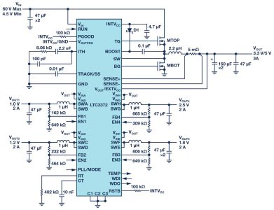
There are different solutions for applications that require conversion from a high input voltage down to a very low output voltage. One interesting example is the conversion from 48V down to 3.3V. Such a specification is not only common in server applications for the information technology market, but in telecommunications as well.Figure 1. Conversion of a voltage from 48V down to 3.3V in one single conversion step.

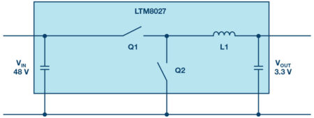
If a step-down converter (buck) is used for this single conversion step, as shown in Figure 1, the problem of small duty cycles emerges. The duty cycle is the relationship between the on-time (when the main switch is turned on) and the off-time (when the main switch is turned off). A buck converter has a duty cycle, which is defined by the following formula:

With an input voltage of 48V and an output voltage of 3.3V, the duty cycle is approximately 7%.
This means that at a switching frequency of 1MHz (1000ns per switching period), the Q1 switch is turned on for only 70ns. Then, the Q1 switch is turned off for 930ns and Q2 is turned on. For such a circuit, a switching regulator has to be chosen that allows for a minimum on-time of 70ns or less. If such a component is selected, there is another challenge. Usually the very high power conversion efficiency of a buck regulator is reduced when operating at very short duty cycles. This is because there is only a very short time available to store energy in the inductor. The inductor needs to provide power for a long period during the off-time. This typically leads to very high peak currents in the circuit. To lower these currents, the inductance of L1 needs to be relatively large. This is due to the fact that during the on-time, a large voltage difference is applied across L1 in Figure 1.
In the example, we see about 44.7V across the inductor during the on-time, 48V on the switch-node side, and 3.3V on the output side. The inductor current is calculated by the following formula:

If there is a high voltage across the inductor, the current rises during a fixed time period and at a fixed inductance. To reduce inductor peak currents, a higher inductance value needs to be selected. However, a higher value inductor adds to increased power losses. Under these voltage conditions, an efficient LTM8027 µModule® regulator from Analog Devices achieves power efficiency of only 80% at 4A output current.
Today, a very common and more efficient circuit solution to increase the power efficiency is the generation of an intermediate voltage. A cascaded setup with two highly efficient step-down (buck) regulators is shown in Figure 2. In the first step, the voltage of 48V is converted to 12V. This voltage is then converted down to 3.3V in a second conversion step. The LTM8027 µModule regulator has a total conversion efficiency of more than 92% when going from 48V down to 12V. The second conversion step from 12V down to 3.3V, performed with a LTM4624, has a conversion efficiency of 90%. This yields a total power conversion efficiency of 83%. This is 3% higher than the direct conversion in Figure 1.

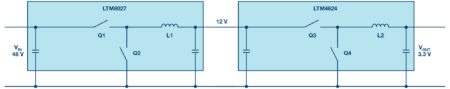
Figure 2. Voltage conversion from 48V down to 3.3V in two steps, including a 12V intermediate voltage.

This can be quite surprising since all the power on the 3.3V output needed to run through two individual switching regulator circuits. The efficiency of the circuit in Figure 1 is lower due to the short duty cycle and the resulting high inductor peak currents.
When comparing single step-down architectures with intermediate bus architectures, there are many more aspects to consider besides power efficiency.
One other solution to this basic problem is the LTC7821, hybrid step-down controller from Analog Devices. It combines charge pump action with a step-down buck regulation. This enables the duty cycle to be 2× VIN/VOUT and, thus, very high step down ratios can be achieved at very high power conversion efficiencies.
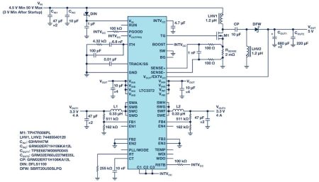
Figure 3 shows the circuit setup of the LTC7821. It is a hybrid step-down synchronous controller. It combines a charge pump to halve the input voltage with a synchronous step-down converter utilising the buck topology. With it, conversion efficiencies of more than 97% for converting 48V to 12V at a 500kHz switching frequency are possible. With other architectures, this high efficiency would only be feasible with much lower switching frequencies. They would require larger inductors.


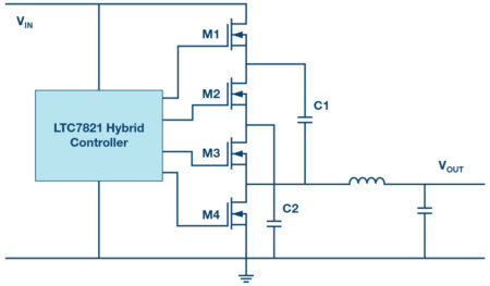
Figure 3. Circuit design for a hybrid step-down converter.

Four external switching transistors are activated. During operation, the capacitors C1 and C2 generate the charge pump function. The voltage generated in this way is converted into a precisely regulated output voltage with the synchronous buck function. To optimise the EMC characteristics, the charge pump is used with soft switching operations.
The combination of a charge pump and a buck topology offers the following advantages. Due to the optimal combination of charge pump and synchronous switching regulator, the conversion efficiency is very high. The external MOSFETs M2, M3, and M4 only have to withstand low voltages. The circuit is also compact. The coil is smaller and cheaper than in a single-stage converter approach. For this hybrid controller, the duty cycle for switches M1 and M3 is D = 2 × VOUT/VIN. For M2 and M4, the duty cycle is calculated as D = (VIN – 2 × VOUT)/VIN.
For charge pumps, many developers assume a power output limitation of approximately 100mW. The hybrid converter switch with the LTC7821 is designed for output currents of up to 25A. For even higher performance, multiple LTC7821 controllers can be connected in a parallel multiphase configuration with synchronised frequency to share the overall load.

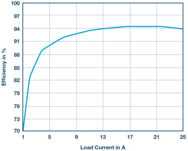
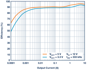
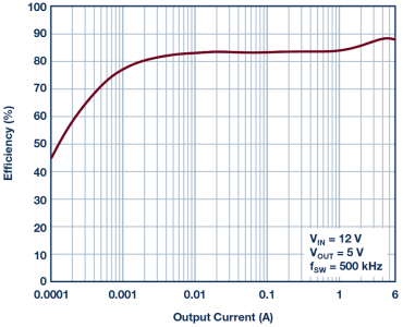
Figure 4. Typical conversion efficiency for converting 48V to 5V at a switching frequency of 500kHz.

Figure 4 shows the typical conversion efficiency for a 48V input voltage and a 5V output voltage at different load currents. At approximately 6 A, a conversion efficiency exceeding 90% is reached. Between 13A and 24A, the efficiency is even higher than 94%.
A hybrid step-down controller supplies very high conversion efficiency in a compact form. It offers an interesting alternative to a discrete two-stage switching regulator design with intermediate bus voltage and to a single-stage converter that is forced to operate at a very low duty cycle. Some designers will prefer a cascaded architecture, others a hybrid architecture. With these two available options, every design should be successful.

Analog Devices: https://www.analog.com

About the Author
Frederik Dostal studied microelectronics at the University of Erlangen-Nuremberg, Germany. Starting work in the power management business in 2001, he has been active in various applications positions including four years in Phoenix, Arizona, working on switch mode power supplies. He joined Analog Devices in 2009 and works as a power management technical expert for Europe. He can be reached at frederik.dostal@analog.com.


> Read More

High voltage boost and inverting converters for communications

The field of electronic communications is rapidly expanding into every aspect of ordinary life. Detection, transmission, and reception of data require a wide array of devices such as optical sensors, RF MEMS, PIN diodes, APDs, laser diodes, and high voltage DACs, to name just a few. In many cases, these devices require several hundred volts to operate, calling for dc-to-dc converters that meet stringent efficiency, space, and cost requirements.

Analog Devices’ LT8365 is a versatile monolithic boost converter that integrates a 150V, 1.5A switch, making it ideal for high voltage applications found in the communications field, including portable devices. High voltage outputs are easily produced from inputs as low as 2.8V and as high as 60V. It features optional spread spectrum frequency modulation, which can help mitigate EMI, and many other popular features detailed in the data sheet.

The converters shown in Figure 1 and Figure 2 have been used to provide the positive and negative voltage rails for high voltage DACs, MEMS, RF switches, and high voltage op amps, from a 12V input source. These converters operate in discontinuous conduction mode (DCM) and deliver as much as 10mA, with +250V and –250V output voltages with a conversion efficiency of about 80%.

Figure 1. 12V input to 250V output 2-stage boost converter.


Figure 2. 12V input to –250V output 2-stage inverting converter.

Step-Up Ratios >1:40
One benefit of DCM operation in a boost converter is the ability to achieve a high step-up ratio independent of duty cycle. Additionally, the values and physical sizes of the inductor and output capacitor can be reduced, which leads to a smaller overall footprint solution on the PCB. The circuit in Figure 3 can easily fit in an area less than 1cm2.
There are situations when only a very low input source is available and a high output voltage is needed. The converter shown in Figure 3 could be used to drive a variety of avalanche photo diodes, PIN diodes, and other devices requiring high bias voltages. This boost converter produces 125V from a 3V input source with up to 3mA of load current.

Figure 3. 3V input to 125V output boost converter.

The converter shown in Figure 4 extends the 125V output to 250V from a 3V input source and supports about 1.5mA. There are many devices in the communications field requiring such high bias voltages from low input voltage sources.

Figure 4. 3V input to 250V output 2-stage boost converter.

How High or Low Can You Go?
For situations where very high voltage is needed, whether positive or negative, a boost converter can use multiplier stages to boost the output 2×, 3×, or more. The converters in Figure 1 and Figure 2 show how to double the switch voltage in both directions, positive and negative. The 3-stage boost converter in Figure 5 delivers 375V at 8mA from a 12V input source.
Note that the available output current must decrease as output voltage increases, since the switch capability does not change. As an example, a single-stage converter designed to deliver 20mA will deliver about 10mA when a second stage is added. As additional stages are added, always ensure the peak switch current stays within the guaranteed switch current limit.

Figure 5. 12V input to 375V output 3-stage boost converter.

Output Voltage Sensing Simplified
The LT8365 offers a single FBX pin to sense the output voltage. A simple resistor divider connected to the FBX pin senses the output voltage, independent of output polarity, as observed on all the schematics presented in this article.
Conclusion
The LT8365 enables applications that require compact, efficient, high output voltage boost conversion from input voltages as low as 2.8V, which is common in the field of communications. It can also be used as an inverting converter and in popular topologies such as CUK and SEPIC converters. The LT8365 is available in a small, thermally enhanced, 16-lead MSOP package.

About the Author
Jesus Rosales is an applications engineer in Analog Devices’ Applications Group in Milpitas, CA. He joined Linear Technology (now a part of ADI) in 1995 as an associate engineer and was promoted to applications engineer in 2001. He has since supported the boost/inverting/SEPIC family of monolithic converters and some offline isolated application controllers. He received an associate degree in electronics from Bay Valley Technical Institute in 1982. He can be reached at jesus.rosales@analog.com.

> Read More

PLL/VCO device delivers groundbreaking low phase noise and spur performance

Increasing demands for frequency bandwidth, throughput, and dynamic range in communications systems, together with the need for higher antenna frequencies used in millimetre wave 5G, have all placed further demands on the quality of the local oscillator (LO) or clock used in communications or mixed-signal systems, respectively.

The integrated phase-locked loop (PLL) and voltage controlled oscillator (VCO), the ADF4371, and the similar ADF4372, showcase Analog Devices’ efforts to address the needs of these demanding applications.


Figure 1. ADF4371 block diagram.

Frequency Coverage
To maximise frequency coverage, the ADF4371/ADF4372 VCO covers an octave range from 4GHz to 8GHz, and, by using frequency dividers at the output, dividing by 1/2/4/8/16/32/64 allows full frequency coverage at the main RF8 output of between 62.5MHz to 8000MHz. A second identical output is provided to allow a user to drive a converter clock. The open-loop VCO phase noise is –109dBc/Hz at 100kHz offset for the 8GHz output frequency.
Until recently, generating high frequencies required the use of external frequency multipliers, typically fabricated on GaAs processes, and they often demanded additional filtering, along with amplification, to overcome the effect of the filtering.
To achieve higher frequencies, the ADF4371/ADF4372 contain an integrated frequency doubler, which provides 8GHz to 16GHz output at the differential RF16 pins. The ADF4371 also features a frequency quadrupler that generates from 16GHz to 32GHz at the RF32 differential output. To minimise the generation of unwanted multiplier products, the ADF4371/ADF4372 contain tracking filters that optimise the power level of the desired frequency while suppressing the unwanted multiplier products. On the doubled output, the VCO feedthrough is –45dBc. On the quad output, the suppression is approximately –35dBc.


Figure 2. RMS jitter at 6.144GHz.

Figure 3. RMS jitter at 12.288GHz.

Leading PLL Performance for Converter Clocks
Improvements to the PLL circuitry mean the ADF4371/ADF4372 devices have a PLL figure of merit (FOM) as low as –234dBc/Hz that, when together with a correspondingly low 1/f noise of –127dBc/Hz (normalised to 1GHz output frequency at 10kHz offset), allows users to generate clocks with an rms jitter number as low as 40fs (1kHz to 100MHz integration limit), making them very suitable for use in the most demanding converter clock applications. A simple low-pass filter with small resistors is recommended in order to minimise the resistor noise, which may appear in the loop. A high frequency (250MHz or 125MHz using the reference frequency doubler) ultralow noise reference source is essential for achieving such low noise. The phase frequency detector (PFD) can operate up to a maximum of 250MHz in integer-N applications. The doubled VCO differential output at RF16 can be used to interface directly to some ADI converters without the need for external balun circuitry, which would increase cost and performance. No degradation in performance from 6.144GHz to 12.288GHz is expected.

Communications and Instrumentation LOs
For wireless and instrumentation applications, the ADF4371/ADF4372 contain 39-bit resolution sigma-delta modulators, which enable frequency generation with sub-millihertz resolution with 0Hz error. In this case, the ADF4371 PFD operates up to a maximum of 160MHz PFD frequency. In these applications, the ADF4371/ADF4372 deliver <48fs rms jitter. The ADF4371 also has industry-leading PLL spurious performance, with PFD spurious as low as –100dBc and in-band, unfiltered integer boundary spurious as low as –55dBc. This performance level greatly simplifies frequency planning and reduces time to market. Many fractional-N PLL and VCO devices have unpredictable fractional-N spurious mechanisms, which can lead to additional unplanned characterisation and frequency planning, which add complexity and cost.

Small Size
The ADF4371/ADF4372 PLL/VCO devices are available in 7mm × 7mm, 48-lead land grid array (LGA) packages. Minimal additional decoupling is required, meaning exceptional performance exists in a small footprint solution.
To achieve the best performance, the use of high quality low dropout (LDO) regulators such as the ADM7150 or LT3045 are recommended. The VCO can be supplied with either 3.3V or 5V, and the remaining circuitry is powered from a 3.3V rail. The ADF4371 can be simulated in ADIsimPLL™ to assist the user in designing the appropriate external component circuitry required to implement a full PLL system.

Conclusion
Industry-leading frequency coverage, performance, and small form factor combine on the ADF4371 to address the high demands of new communication and instrumentation systems.

About the Author
Ian Collins graduated from University College Cork with a degree in electrical and electronic engineering, and he has worked in the RF and Microwave Group at Analog Devices since 2000. He is currently an applications manager in the Microwave Frequency Generation Group, which focuses mainly on phase-locked loop (PLL) and voltage controlled oscillator (VCO) products. When not spending time at work or with his young family, Ian enjoys photography and the theatre (both on- and off-stage), reading, and listening to music. He can be reached at ian.collins@analog.com.

> Read More

All-in-One power solution for automotive infotainment – single IC produces five rails directly from battery

Our connected and media driven lifestyles are a result of, or a reason for, technology’s push into every aspect of our lives, including today’s highly integrated automotive infotainment systems. The complex mix of electronic components contained in automobile infotainment systems mirrors consumer electronics: high performance microcontrollers, memory, interface, and driver ICs. The power supply picture is just as complex, as each component may require a variety of low voltage rails with wide ranging power requirements. Complexity is not limited to the infotainment systems. Automotive performance, fuel efficiency, and driver convenience features require increasingly advanced electronic systems. The power system also stands between sensitive electronics and the unwelcoming conditions of the automotive setting – namely the wide-ranging voltage and predictably transient battery environment serving as input. A well-designed power system must both power and protect electronics, even as manufacturers make the automotive environment less inviting to electronics with features such as start-stop technology.

Start-stop technology magnifies the extreme conditions that electronics must face, specifically through repeated engine cranking. A start-stop enabled car restarts the engine repeatedly, but critical systems must remain operational even as the battery supply goes through a cold crank each time – while not catastrophic, a driver suddenly singing acapella as the car’s music goes silent may not add to the car’s positive reviews.

At the other end of the spectrum, ultralow quiescent current is a critical requirement of automobile power systems. An automobile may need to sit unused for a month or more as critical always-on electronic systems quietly run, without draining the battery.

Analog Devices’ LTC3372 all-in-one high voltage controller is capable of maintaining regulation through the extreme voltage changes presented by automotive battery environments. It can keep always-on components running without draining the battery because of its ultralow quiescent current. The LTC3372 features four configurable monolithic regulators and can provide up to five output channels for infotainment or other electronic systems.

Automotive Multichannel Power
The LTC3372 significantly reduces the number of components required to produce multiple rails. It combines proven high voltage automotive controller technology with four configurable monolithic bucks to create a space- and cost-efficient automotive multichannel power solution.

The high voltage buck controller input operates through input surges up to 60V, such as those seen during a load dump, and can also regulate through input dips as low as 4.5V in a standard buck configuration, and down to 3V in a SEPIC configuration. This operating input range enables uninterrupted power to sensitive electronics in the face of significant transients. The LTC3372’s four low voltage bucks are configured independently by combining power stages from a selection of eight 1A power stages. Stages are combined to meet the power requirements of each regulator, with eight possible unique 4-output channel configurations, all directly from an automotive battery source.

One benefit of a single IC multichannel power solution is shared internal voltage references and bias supplies. This bias sharing enables lower per channel IQ specifications for multichannel power than would be available with independent ICs. For a single-channel, always-on supply, the VIN referenced bias IQ is 23µA typical and 46µA maximum at 150°C. With all 5 channels regulating in Burst Mode® operation, the typical bias current is only 60µA total, or 12µA per channel. The LTC3372 enables new always-on applications when its total bias IQ for 5 channels is comparable to a single channel using older technology.

Single-Chip Controller and Regulators
The LTC3372 is a front-end 60V high voltage (HV) buck controller plus four low voltage (LV) 5V monolithic buck regulators with low IQ Burst Mode operation. By integrating a controller and monolithic regulators, LTC3372 can provide up to five separate rails from high input voltage in compact size at low cost. The output voltage of the HV controller can be selected between 3.3V and 5V depending on the level of VOUTPRG pin; the output voltages of the LV regulators can be individually programmed with external resistors through FB1 to FB4 pins.

Figure 1. Typical 60V input application of LTC3372. The HV controller feeds quad 2A, 1V/1.2V/1.8V/2.5V LV regulators. The 3.3V/5V HV controller output can be used as an additional 3A current rail.
Figure 1 and Figure 2 show a typical application and the corresponding efficiency of the HV controller. While the HV controller is typically used for feeding the LV regulators, each regulator operates independently via per channel enable and input pins. Additional flexibility is provided by the eight power stages. The eight switches can be distributed among the LV regulators, with the combination digitally configured through the C bit (C1, C2, C3) to meet rail-specific maximum current limits. Table 1 shows C bit settings and the resulting maximum current limit configurations per regulator number. Figure 3 shows how efficiency varies with the number of switches combined in parallel.


Figure 2. Burst Mode operation efficiency vs. output current of HV controller in Figure 1. The output current is shown up to 10A, which is sufficient to feed four fully-loaded LV regulators and a 3A, 3.3V/5V load.

Figure 3. Burst Mode operation efficiency vs. output current of LV regulators. A 1A, 2A, 3A, and 4A buck represents different configurations when one, two, three, and four switches are connected in parallel.

Table 1. LV Regulator Configurations Are Set via C1, C2, and C3 Codes; In Any Configuration of Less Than Four LV Regulators, the Unused Regulators Enable Pins and Feedback Pins Are Connected to Ground

The LTC3372 also provides an on-chip temperature sensor and watchdog timer features. The temperature sensor allows users to closely monitor die temperature whenever a LV regulator is enabled. The watchdog timer issues a reset signal if the microprocessor fails to clear the timer when malfunction occurs.
Power Loss Optimisation
Often, dc-to-dc converters are judged on their efficiency and are therefore designed to maximise that parameter, but optimising dc-to-dc converters in terms of power loss (instead of just efficiency) usually pays higher performance dividends in high power applications. For a multistage converter system, such as can be created with the LTC3372, efficiency measurements can be misleading when some part of the efficiency is the composite of HV controller and LV regulators.
Keep in mind that power loss optimisation does not mean simply minimising total power loss, but also balancing the distribution of the losses across devices. A good approach is to begin with the LV regulators, as the total power loss across all LV regulators accounts for most of the loss in the LTC3372 system. By considering all applicable LV regulator configurations, a designer can compare a significant range of power loss options. Table 2 lists all applicable configurations and the associated power loss in a 1.2V, 1.8V, 2.5V application at 3A, 3A, 0.5A maximum load, respectively. The difference between the best and the worst configurations is 0.432W. In normal cases, recursively allocating the largest possible switch to the highest power channel yields the best result.

Table 2. Total Burst Mode Operation Power Loss in LV Regulators of 1.2V (3A), 1.8V (3A), 2.5V (0.5A) in Various Configurations; VINA–H are 3.3V and Switching Frequency is 2MHz; The Best Configuration Yields 0.432W Less Power Loss Compared to the Worst Case

More generic efficiency optimisation procedures can be applied to the HV controller. The slight difference is that all/part of the HV controller’s loading becomes the input referred current of LV regulators. When LV regulators are the only loads, the HV controller sees a moderate load, even if each LV regulator is fully loaded. Instead of selecting the low RDS FETs or pursuing the highest peak efficiency, designers should focus on the operating current range of interest. The efficiency vs. output current curves of three FETs with distinct RDS are shown in Figure 4. For the LV regulators in Table 2, using the highest RDS but lowest QG FET yields the highest efficiency in the range below maximum load (3.759A in the optimum configuration).

Figure 4. Burst Mode operation efficiency vs. output current with three different FETs in the HV controller. The same FET for both top and bottom are used. The figure is zoomed into 1A to 6A range to closely observe any crossover to determine the optimum FET for LV regulators in Table 2. 3.759A is the maximum load current when LV regulators are fully loaded. The results suggest that the best selection is the highest RDS but lowest QG FET (BSZ099N06LS5).
SEPIC Controller
In automotive applications, cold crank remains a challenge to dc-to-dc converters. Buck converters are forced to operate in dropout if the regulated output voltage is higher than the input in cold cranking situations. Two alternative front-end topologies, boost and SEPIC, can be realised using available resources provided in the LTC3372’s HV controller to avoid dropout operation.
Even though the boost is slightly simpler, it passes any high voltage input surge to the following buck stage. This precludes the use of high efficiency low voltage buck regulators as the second step-down stage. In Figure 5, we configure the LTC3372 HV controller in a non-synchronous SEPIC topology. The SEPIC converter generates a 5V intermediate rail to power two 3.3V/4A LV regulators and to sustain the continuous operation of HV controller.
When two 4A LV regulators are fully loaded, more than 5A of current is drawn from the SEPIC output. The peak current through the sense resistor can easily exceed 10A as the switch current is the summation of both inductor windings. Considering that the sense resistor is within the hot loop, some effort is required to produce a clean waveform at the current comparator inputs. One solution is to incorporate a differential filtering scheme as shown in the SEPIC schematic, and use a low inductance resistor fabricated in a reversed package.
Figure 6 shows SEPIC efficiency in Burst Mode operation and Figure 7 shows the SEPIC output voltage when a 12V-to-3V transient is applied to the input. Designers should not overlook the heat generated in the catch diode during PCB design. Thermal limits can be met by reserving extra space for a moderately oversized diode and using thicker copper. Another diode and a filtering capacitor are connected to the VIN pin to avoid reversed current and sudden voltage spike due to input transients.

Figure 5. A 4.5V to 50V input non-synchronous HV SEPIC converter feeding two 3.3V/4A LV regulators. After start-up, the SEPIC converter can maintain 5V at VOUT with 3V minimum VIN when two LV regulators are fully loaded. Minimum VIN down to 1.5V is possible if a lighter load is placed on the SEPIC. The output of the SEPIC must be set to 5V to sustain continuous operation when VIN is below 5V. DIN and a 1µF capacitor are connected to the IC VIN to prevent reverse current and transient spike. A differential current sense scheme and low inductance sense resistor are recommended to provide a clean signal at the current comparator inputs. Low inductance (LHV1 and LHV2), maximum switching frequency, and low bandwidth are compromises between right-half-plane zero and current ripple.

Figure 6. Burst Mode operation efficiency vs. output current of non-synchronous SEPIC controller in Figure 5. The output current is shown up to 6A, which is sufficient to feed two fully-loaded 3.3V/4A LV regulators.

Figure 7. Output response of the SEPIC to an input transient similar to a cold crank condition. The input steps down from 12V to 3V within 2ms and stays at 3V for one second before recovering to 12V. Larger ripple is observed during the 3V transient, which is caused by the higher peak current flowing to the output capacitor through the catch diode. The waveforms are taken with two fully loaded 3.3V/4A LV regulators and 500kHz SEPIC switching frequency.
Conclusion
The LTC3372 provides a single chip solution for high voltage multichannel buck converters. Its low IQ operation and low cost per channel are a good fit for always-on systems in automotive applications.

About the Authors
Jin-Jyh Su joined Linear Technology, now part of Analog Devices, as an analogue IC design engineer after graduating from the Georgia Institute of Technology. He was with the Linear Analog Device Power Group in Milpitas, California and Dallas, Texas for 3 years. Su specialises in high performance dc-to-dc converter design. His design experience includes monolithic and controller products operating at high voltage (100V), high speed (3MHz), and low IQ for automotive applications. Su recently joined the Battery Management System (BMS) Group in Dallas, Texas where he is working on multicell battery stack monitors. He can be reached at jin.su@analog.com.
Terry Groom is a power design section leader and has been with Analog Devices for almost 13 years. He is a graduate of Texas A&M and Georgia Institute of Technology. Groom’s design group, located in Dallas, Texas, specialises in high performance dc-to-dc power controllers. He and his team have developed products with voltage inputs from 5V to 150 in multiple switch mode topologies with switching frequencies of up to 3MHz. Groom has more than 30 years of direct design experience in a variety of analogue disciplines. He is proud to be a valued member of the Analog Devices’ Power by Linear development team. He can be reached at terry.groom@analog.com.


> Read More

About Smart Cities

This news story is brought to you by smartcitieselectronics.com, the specialist site dedicated to delivering information about what’s new in the Smart City Electronics industry, with daily news updates, new products and industry news. To stay up-to-date, register to receive our weekly newsletters and keep yourself informed on the latest technology news and new products from around the globe. Simply click this link to register here: Smart Cities Registration