Automotive USB Type-C Power Solution: 45W, 2MHz Buck-Boost Controller in a 1 Inch Square

USB Type-C is a relatively new, high power USB peripheral standard used in computer and portable electronic devices. The USB Type-C standard has driven changes in the USB power delivery specification, allowing for increased bus voltages (up to 20V) and current delivery capability (up to 5A) from the long-standing 5V USB standard. Connected USB-C devices can recognise each other and negotiate a bus voltage – from the default 5V USB output to several higher preset voltage steps – for faster battery charging and higher power delivery where needed, up to 100W.

The simple, compact buck regulators and linear regulators used in battery chargers that require only USB 5V at 500mA to 2A do not sufficiently cover the full range of Type-C USB power. The increased voltage range, 5V to 20V, of Type-C USB power delivery requires more than just step-down voltage conversion from 9V to 36V (or 60V) automotive batteries, or other charging sources. An adjustable buck-boost converter is needed with the ability to both step-up and step-down the input-to-output voltage.

Additionally, for high power automotive USB chargers, a buck-boost converter should support a 10A or higher peak switch current rating and offer low EMI performance. The ability to set the switching frequency outside the AM radio band and maintain a small solution size are sought-after features. High voltage monolithic converters (with onboard switches) are not capable of sustaining such high peak switch currents without burning up.

The LT8390A is a unique 2MHz, synchronous 4-switch buck-boost controller. At 2MHz switching frequency, it can deliver output voltages between 5V and 15V (up to 45W at 3A) to provide power to a connected USB-C device from a car battery. This high controller switching frequency keeps the solution size small, the bandwidth high, and the EMI outside of the AM radio band. Both spread spectrum frequency modulation and low EMI current-sense architecture help LT8390A applications pass the rigors of the CISPR 25 Class 5 automotive EMI standard.

High Power Density Conversion: Size (and Power), Efficiency, Heat

The design of a voltage regulator system operating in an automotive or portable electronics environment is constrained by the space required for the circuit, as well as the heat it generates during operation. These two factors impose an upper bound of achievable power levels while operating within the given design constraints.

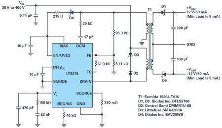
Increasing the switching frequency of a design allows for the use of smaller inductors, which is often the largest footprint component in wide input voltage 4-switch buck-boost voltage regulator designs. The LT8390A’s 2MHz switching frequency capability enables the use of a much smaller inductor size than a 150kHz or 400kHz design. A complete design is shown in Figure 1. Along with a smaller inductor, this solution uses only ceramic output capacitors, eliminating the need for bulky electrolytic capacitors. All the components necessary for this design, including the IC, are contained within a small, 1″ inch square footprint, as shown in Figure 1.

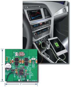
Figure 1. Efficient, low EMI USB Type-C power solution that fits in a 1″ square.

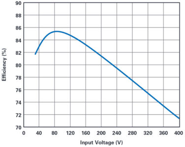
Figure 2 shows a 45W LT8390A solution using AEC qualified components. This design experiences a maximum temperature increase of 65°C from the ambient temperature, as shown in Figure 3. Even with the small solution size, the LT8390A system boasts a peak efficiency of 94% while delivering a 45W output, and deviates in efficiency by less than 10% over the input range for each output voltage created, shown in the graphs in Figure 4.

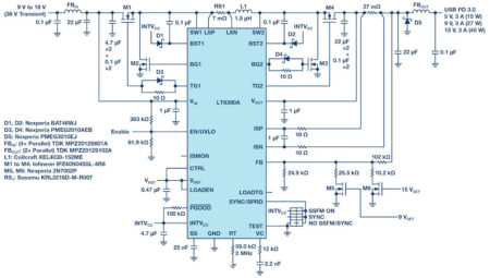
Figure 2. This LT8390A voltage regulator solution provides up to 3A at selectable 5V, 9V, or 15V low EMI outputs using AEC qualified

MOSFETs, magnetics, and capacitors.

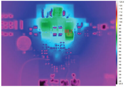
Figure 3. While generating 45W of output power, this small circuit’s greatest temperature rise is only 65°C above ambient temperature.

Low EMI for Automotive Applications

The LT8390A has several unique EMI mitigating features that enable high power conversion with low noise performance, which simplifies its implementation in automotive systems. A notable difference between LT8390A and alternative 4-switch controllers is the placement of the inductor current sensing resistor. Most 4-switch buck-boost controllers tend to use a ground-referred current sensing scheme to obtain switch current information, whereas the LT8390A places its current sense resistor in-line with the inductor. By placing the sensing resistor in-line with the inductor, it is effectively removed from both the buck and boost hot loops, shrinking the loops in size and improving the EMI performance.

Along with the architectural advantage of the inductor sensing resistor placement, the LT8390A has built-in spread spectrum frequency modulation to further reduce EMI generated by the controller. Furthermore, the switching edge rate is controlled on both the buck and boost power switches using only a few discrete components to slow the turn-on of the MOSFETs, ensuring the proper balance of high frequency EMI reduction and temperature rise in the power switches. With these EMI-reducing features, the only filtering needed to meet CISPR 25 compliance is taken care of by small ferrite filters on the input and output rather than large ferrite cases and bulky LC filters. The solution shown in Figure 1 was designed using only AEC-Q100 components.

Seamless Output Voltage Transitions

The LT8390A’s output voltage can be adjusted without shutting down the converter by using logic-level signals to drive MOSFETs that adjust the resistor divider off the output to change the set voltage. A USB PD source controller device with GPIO pins can be used in conjunction with the LT8390A system to facilitate the negotiation process between host and USB-connected device and to set the desired bus voltage.

Figure 5 demonstrates how smoothly the output of the LT8390A system transitions from one output voltage to another. When powered from a 12V input source, each transition to an increased output voltage takes at most 150µs to settle, as measured from the rising edge of the digital control signal. During these changes in the output voltage, the buck-boost controller goes through mode transitions – between buck, boost, and buck-boost operation – depending on the relation of input to output voltages. These mode transitions are performed in a controlled manner, preventing excessive overshoot or sagging of the output voltage.

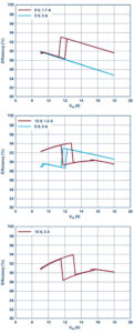
Figure 4. The LT8390A voltage regulator system remains in the 94% to 84% efficiency range across all output voltages generated when powered from an automotive SLA battery.

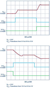
Figure 5. The output of the LT8390A system smoothly transitions between 5V, 9V, and 15V outputs while maintaining continuous power deliver to the output.

Expanding Beyond 45 W

To push the output power level beyond 45W requires operating at a lower switching frequency to reduce switching losses, which might otherwise thermally stress the MOSFETs at this power level. As an alternative to the LT8390A, the LT8390 operates between 150kHz and 600kHz with the same feature set as LT8390A – allowing low EMI, high power buck-boost designs. A 400kHz LT8390 system, utilising a larger inductor and output capacitor, easily achieves 100W of output power from an automotive battery input with acceptable temperature rise. Figure 6 illustrates the power capabilities of the LT8390A and LT8390 product line from various battery-powered inputs.

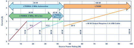
Figure 6. The LT8390A and LT8390 cover a wide range of output power levels for USB power delivery.

Conclusion

The new USB standard for voltage regulators powering connected devices permits higher power transfer by increasing the output voltage range and current delivery that regulators can provide. Portable and automotive battery-powered USB-C charger devices require a wide VIN/VOUT buck-boost regulator to deliver a bus voltage above or below the input voltage. The LT8390A provides up to 45W of output power in a small footprint, made possible by its 2MHz switching frequency. For power levels exceeding 45W, the LT8390 can be used with a slightly larger solution size and lower switching frequency.

By Kyle Lawrence

Kyle Lawrence [kyle.lawrence@analog.com] is an applications engineer at Analog Devices. He is responsible for the design and testing of a variety of dc-to-dc converters, including 4-switch buck-boost voltage regulators and LED drivers targeting low EMI automotive applications. Kyle received his B.S. degree in electrical engineering from the University of California, Santa Cruz in 2014.


> Read More

LED installation beacon is available in seven colours

Available in a choice of seven colours, the LED installation beacon 240 Multicolour has UL approval and is rated IP69K, the highest protection rating, said Werma Signaltechnik.

The compact LED installation beacon also has UL approval required for the USA. Colour options are red, yellow, green, white, blue, purple and turquoise.  The UL certification enables it to be used worldwide, conforming to the safety regulations of the USA and Canada.

The IP69K standard is the highest protection class for electrical equipment, guaranteeing protection against solid objects, liquids, steam and dust. Water penetration is not possible, even at short distances, very high pressure, and high temperatures, ensuring it can be used with high-pressure systems.

Typical application examples are the mobile machinery, food processing, pharmaceutical and petrochemical industries, where all equipment must meet washdown requirements and be regularly exposed to high-pressure water jets.

The LED installation beacon 240 Multicolour combines a large, bright and attention-grabbing illuminated surface with excellent visibility and robustness. It has a diameter of 55mm and rises just 46mm above the surface when installed, making it suitable for use where installation space is limited.

The seven colours allow it to be used in a variety of ways. For example to signal malfunctions or statuses at the control console of a machine, in the machine housing or on control cabinets. The compact size means it is suitable for automation applications.

The LEDs signal is clearly visible from all angles, said Werma, yet thanks to the frosted dome, the light effect is pleasant and homogenous. The efficient installation beacon needs only 40 to 130mA, depending on the variant.

The beacon can also be supplied in combination with a buzzer which emits a 3,400Hz pulse tone signal with a volume of 85dB.

The M30 installation size means the signal device can be easily mounted. Bit-encoded controlling allows the three basic colours green, yellow and red to be displayed using just two PLC outputs. With additional outputs, blue, turquoise, violet and white can also be activated.

The beacon has a long service life of up to 50,000 hours, added Werma.

http://www.werma.com

> Read More

Single IC Can Produce Isolated or Nonisolated ±12 V Outputs from 30 V to 400 V Input

Electric vehicles, large-scale battery storage stacks, home automation, industrial, and telecom power all require converting high voltages to ±12 V, where dual polarity rails are required for powering amplifiers, sensors, data converters, and industrial process controllers. One challenge in all of these systems is creating a compact, efficient dual polarity regulator that can operate over a temperature range of –40°C to +125°C—especially important in automotive and other high ambient temperature applications.

Linear regulators are well understood and typically top the list of candidates for bipolar supplies, but are not suitable in the high input voltage, low output voltage applications previously mentioned, mainly due to heat dissipation in the linear regulator at high step-down ratios. Furthermore, a dual polarity solution requires at least two integrated circuits (ICs): one positive output linear regulator and a negative converter. A better solution would use a single switching regulator that produces both outputs from a relatively high input, at good efficiency and regulation, while fitting tight spaces and reducing cost.

This article presents two elegant circuits that generate ±12 V outputs from a wide 30 V to 400 V input voltage range, both using a single high voltage LT8315 converter. One circuit is an isolated flyback topology; the other is based on a nonisolated buck topology. The LT8315 itself is a high voltage monolithic converter with integrated 630 V/300 mA MOSFET, control circuitry, and high voltage start-up circuit, inside a thermally enhanced 20-lead TSSOP package.

Isolated Dual Polarity Flyback Regulator with No Optocoupler

Flyback converters are widely used in multi-output applications to provide galvanic isolation, improve safety, and enhance noise immunity. Outputs can be positive or negative, depending on which side of the output is grounded. Traditionally, the output voltage regulation is achieved using optocouplers to transfer information from the secondary-side reference circuitry to the primary side. The problem is that optocouplers add significant complexity and degrade reliability due to propagation delay, aging, and gain variation, etc. Typically, the one output connected to the feedback pin of the IC dominates the regulation loop, while other outputs are loosely controlled through the transformer windings, resulting in poor regulation of those outputs.

The LT8315 requires no optocoupler and samples the reflected, isolated output voltage from a tertiary winding on the power transformer. Also, the output voltage is sensed when the secondary current is almost zero to achieve excellent load regulation. In a dual output design, this unique sensing scheme allows each output to be closely regulated—both outputs can dominate the regulation. As a result, a typical ±5% load regulation is easily achieved.

The LT8315 solution shown in Figure 1 operates under quasi-resonant boundary conduction mode. The primary MOSFET has a minimum turn-on loss because the MOSFET turns on when the switch node rings to its valley. There is no diode reverse recovery loss on the secondary side. A 3 kV reinforced insulation transformer is the only component across the isolation barrier, enhancing system reliability and meeting stringent high voltage power isolation requirements. Figure 2 shows the full load efficiency curve under different input voltages. This flyback converter achieves 85.3% peak efficiency when the input is 70 V and both load currents are 50 mA.

Figure 1 shows the complete schematic of a flyback converter with a wide input range from 30 V to 400 V. It outputs ±12 V and maintains tight regulation with load currents from 5 mA to 50 mA. This flyback converter has 85.3% peak efficiency, as shown in Figure 2.

Figure 1. A complete ±12 V/50 mA isolated flyback converter for a wide input range, 30 V to 400 V.

Figure 2. Full load efficiency vs. input voltage for the flyback converter in Figure 1.

Figure 3. Schematic of a nonisolated dual inductor buck converter using a single LT8315 IC: 30 V to 400 V input to ±12 V outputs at 30 mA each.

Nonisolated Dual Polarity Buck Regulator with Two Inductors

The LT8315’s high voltage input ability can be applied in nonisolated solutions by using off-the-shelf inductors. A buck regulator with dual inductors, requiring only a few components, is shown in Figure 3. This converter accepts an extremely wide-ranging input—30 V to 400 V—and produces ±12 V/30 mA outputs. This circuit can achieve efficiency as high as 87% at full load for both outputs with a 30 V input.

In this topology, LT8315’s GND pad is intentionally ungrounded and connected as the common switch node for driving both outputs. For PCB layout, LT8315’s GND pad’s size should be constrained within the exposed pad area to reduce electromagnetic interference to other components because the GND trace is a relatively noisy switch node in this topology. Diode D2 and two 1% resistors at the FB pin form the feedback path regulating the positive output voltage. D2 is necessary to prevent the FB pin discharging whenever the MOSFET conducts. The resistive voltage divider does not need to take into account the forward voltage drop of D2 because the forward voltage of D2 and D3 are equal and cancel; therefore, the feedback network tracks and closely regulates the positive output voltage.

The negative rail comprises a low voltage coupling capacitor CFLY, a second inductor L2, a catch diode D4, and the negative output capacitor CO2. According to the inductor volt-second balance for the circuit loop of CO1-L1-CFLY-L2, the average voltage across L1 and L2 is zero, so the coupling capacitor CFLY’s voltage is equal to the positive output voltage. CFLY charges up L2 during the on-time of the MOSFET, while D4 provides a path for the L2 discharge during the MOSFET off-time. The negative output voltage is indirectly regulated based on the voltage of CFLY remaining constant and equal to the positive output voltage. As shown in the regulation curve of Figure 4, the negative supply maintains ±5% regulation for a load range of 3 mA to 30 mA at various input voltages, when the positive load is at a full 30 mA.

Figure 4. Negative 12 V load regulation curves at various input voltages for the dual inductor buck converter in Figure 3.

Conclusion

This article presents two dual polarity converter solutions for a wide 30 V to 400 V input range: one isolated, the other nonisolated. The LT8315 is used in both, due to its high voltage integrated MOSFET, no optocoupler feedback loop, and internal high voltage startup circuit. Other features include low ripple Burst Mode® operation, soft start, programmable current limit, undervoltage lockout, temperature compensation, and low quiescent current. LT8315’s high level of integration simplifies the design of high voltage input and dual polarity output circuits for a wide variety of applications.

About the Author

Zhijun (George) Qian is a senior engineer at Analog Devices. He is responsible for power product applications of various nonisolated and isolated converters. He obtained his B.S. and M.S. from Zhejiang University, and his Ph.D. from University of Central Florida, all in power electronics. He joined Linear Technology (now part of ADI) in 2010. He can be reached at george.qian@analog.com.

About the Author

William Xiong graduated from Cal Poly, San Luis Obispo in 2017 with a bachelor’s degree in electrical engineering. He started working at Analog Devices as an applications engineer in July 2017 and works with buck, boost, and isolated topologies such as flyback and forward converters. He can be reached at william.xiong@analog.com.

> Read More

Semtech Collaborates with Communicate2Integrate for Smart Plant Care Solution, “Florja”

Semtech Corporation has announced that Communicate2Integrate GmbH, an intelligent Internet of Things (IoT) company based in Munich, Germany, has chosen to integrate Semtech’s LoRa® devices and LoRaWAN® connectivity for its Florja solution. Florja is a Cloud-based plant management platform that allows users to monitor the current status of their plants from anywhere. Florja sensors enabled by LoRa and using LoRaWAN connectivity can monitor for the temperature, humidity and salt level found in the soil which then relays the data to the Florja platform accessible via desktop and smartphones for further intelligent analysis.

“Florja is innovating toward a new and easier way to manage plants,” said Michael Urban, chief executive officer of Communicate2Integrate. “Moreover, Florja is scalable from the everyday home plant enthusiast to large scale businesses that need real-time information, automated and intelligent plant care advice or a smart irrigation system. No matter how the platform is used, LoRaWAN is providing that necessary plant data in real time, combined with internal know-how and external data to maintain its health.”

According to a 2020 McKinsey article, advanced technology such as connected sensors “could further increase yields, improve the efficiency of water and other inputs, and build sustainability and resilience across crop cultivation and animal husbandry.” With a renewed focus on sustainability for businesses and consumers, the plug and play Florja platform is an ideal solution for smart plant care for environmentally conscious users. The Florja system includes LoRa-enabled sensors utilising LoRaWAN to measure temperature and humidity in soil and air, electrical conductivity in soil and light irradiation as well as a Florja Cloud platform for users to remotely view that data.

“Semtech’s LoRa devices and LoRaWAN are a complementary fit for the smart agriculture industry,” said Marc Pégulu, vice president of IoT product marketing and strategy for Semtech’s Wireless and Sensing Products Group. “The long range coverage coupled with low power usage of the technology is making the lives of farmers and plant growers much easier and smarter.”

To learn more about Florja, please visit here.

Information on how Semtech’s LoRa devices are innovating smart agriculture can be found here.

> Read More

About Smart Cities

This news story is brought to you by smartcitieselectronics.com, the specialist site dedicated to delivering information about what’s new in the Smart City Electronics industry, with daily news updates, new products and industry news. To stay up-to-date, register to receive our weekly newsletters and keep yourself informed on the latest technology news and new products from around the globe. Simply click this link to register here: Smart Cities Registration