Accurate, Low Power Remote Sensing Ideas

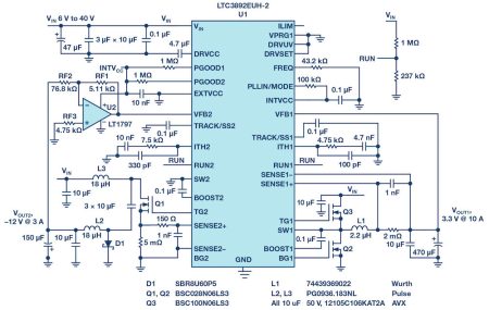
The remote sensing examples shown here feature high reliability, easy connectivity, and very low power. These circuits target industrial settings that require robust communications and minimal battery maintenance. The solutions combine recent advances in low power, high precision amplification with comparably low power, high reliability wireless mesh network capability. Enabling the solutions are the LTC2063 zero-drift, low input bias amplifier, which runs at 2µA max, and the LTP5901-IPM, which consumes less than 1.5µA in sleep mode. The power dissipation for these devices is low enough that they can run from a benchtop-made battery comprised of copper and zinc electrodes, each four inches square in area, and an electrolyte consisting of the pithy innards of a lemon.

Wireless Mesh

Measurements performed and retrieved on a wireless network in industrial settings rarely require high speeds, but they usually require high reliability and security, in addition to low power operation to maximise battery operating time. The LTP5901-IPM forms a node, or a SmartMesh® IP Mote, in an 802.15.4e wireless network. The LTP5901-IPM integrates a 10-bit, 0V to 1.8V ADC alongside an internal ARM® Cortex®-M3 32-bit microprocessor, which enables sensing with easy programmability. This mote is designed for security, reliability, low power, flexibility, and programmability.

Four Sense Applications

Overall, the design of the following circuits did not require rocket science. Yet, they are tidy, efficient, and well-tailored to specific applications. Complexity is not required and, in fact, would be a cost and reliability hazard.

Each circuit engages a sensor at the input and processes the sensor output to produce an output voltage. With the LTP5901-IPM 10-bit ADC as an input, each circuit tries to map the input to capture much of the 0V to 1.8 Vrange.

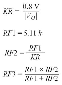
Basic Battery Voltage Sense

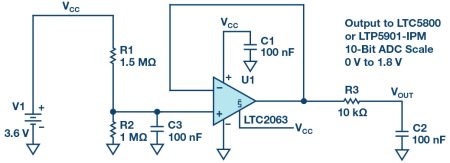
Figure 1. Simple battery voltage sense.

Figure 1 shows a typical noninverting unity-gain negative feedback op amp configuration that senses a divided-down voltage. The ADC range on the LTP5901 input is 0V to 1.8V. R1 and R2 divide down the battery voltage with minimal quiescent current to enable long lasting battery life. The input bias current of the LTC2063 is low enough that even these large resistance values do not affect the final 10-bit ADC accuracy. The LTC2063 consumes minimal supply current and provides the advantage of zero-drift vs. time and temperature.


Current Sense

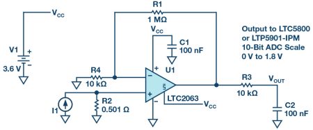
Figure 2. Current sense circuit.

The beauty of battery-powered and isolated electronics is the ability to place ground anywhere. One can sense a current in the most convenient circuit topology without loss of generality, while placing the terminals anywhere relative to local ground. For unipolar current such as a 4mA to 20mA industrial loop, one can safely sense relative to local ground using a traditional low-side topology. Figure 2 shows the current flowing through a very small resistor R2, which develops a sense voltage. This input voltage can be extremely small due to the amplifier’s zero-drift, very low valued offset voltage performance. The circuit shown gains up the input developed across a 501mΩ sense resistor by 101V/V. At 20mA, the VOUT is 1.012V. Other values can be chosen to maximise the use of the ADC’s 1.8V range.

Resistance R4 is relatively low and acts as a low impedance shunt of LTC2063 input capacitance. As a consequence, interaction between the large R1 feedback resistor and input capacitance does not play into stability.

The circuit as constructed is optimised for test current ranges from 0mA to 35mA, mapping to the 0V to 1.8V ADC range.

Irradiance Meter

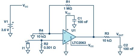
Figure 3. Irradiance measurement using a solar cell in short circuit.

The circuit of Figure 2 can also be used to measure the short-circuit current of a solar cell. Silicon and other solar cells are highly linear in current vs. irradiance when operated in the short-circuit current mode. Short-circuit current is the current from a solar cell with 0V across. The circuit in Figure 3 does not keep the solar cell at precisely 0V at maximum current; however, even with 20mA in full sunlight, the voltage is only 10mV. A 10mV level across the solar cell is virtually a short on its I-V curve.

One might imagine a transimpedance amplifier (TIA) instead. A TIA can force 0V across the solar cell and measure current. The trouble with this kind of circuit is that the op amp supplies the solar cell’s current across the entire range of irradiance. When the priority is minimum power dissipation of the remote sense circuit, 20mA from the battery through the op amp is unacceptable.

Given the need to remain near 0V, a small sense resistor should be used. A remotely located, battery-powered sense of small voltages once again suggests the use of a very accurate, low power amplifier such as the LTC2063.

Solar installations result in exactly the sorts of physical layouts that demand wireless mesh networking with zero temperature drift measurement. Fortunately, silicon photodiodes, in the short-circuit condition, are fairly stable vs. temperature. A simple and robust design utilising the LTC2063 and LTP5901-IPM, combined with a silicon solar cell, is the ideal solution to sensing across a large installation field with changing ambient temperature conditions.

Temperature Measurement with Thermocouple

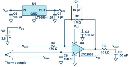
Figure 4. Thermocouple sense circuit.

Thermocouple voltages can be positive or negative. The circuit of Figure 4 combines the use of a micropower reference and a micropower amplifier to sense tiny voltages that are both positive and negative. It is fortunate that a thermocouple, if electrically isolated from its device under test (DUT), can be placed at whatever voltage domain is convenient. The example in Figure 4 biases the thermocouple at 1.25V by using the LT6656-1.25. The circuit output is a very highly gained version of the small thermocouple voltage on top of a 1.25V reference. The ADC range of 0V to 1.8V is a reasonable target for this configuration. The extremely high gain of roughly 2000V/V would not be feasible without the employment of a zero-drift, low offset amplifier.

Conclusion

Extremely low power, accurate, remote sensing is absolutely attainable. The examples shown in this article reveal the simplicity of combining a low power, high accuracy amplifier with a programmable system-on-chip wireless mesh node.


About the Author

Aaron Schultz is an applications engineering manager in the LPS business unit. His multiple system engineering roles in both design and applications have exposed him to topics ranging across battery management, photovoltaics, dimmable LED drive circuits, low voltage and high current dc-to-dc conversion, high speed fiber optic communication, advanced DDR3 memory R&D, custom tool development, validation, and basic analog circuits, while over half of his career has been spent in power conversion. He graduated from Carnegie Mellon University in 1993 and MIT in 1995. By night he plays jazz piano. He can be reached at aaron.schultz@analog.com.

> Read More

Renesas embraces Microsoft Visual Studio Code across its entire MCU and MPU lineup

Renesas Electronics Corporation has announced that customers can now use Microsoft® Visual Studio Code (VS Code) to program the complete line of Renesas microcontrollers (MCUs) and microprocessors (MPUs). Renesas has added tool extensions for all of its embedded processors to the Microsoft VS Code website, enabling a huge base of designers comfortable with the popular Integrated Development Environment (IDE) and code editor to work in their preferred environment.

The popular VS Code IDE simplifies and accelerates code editing across a variety of platforms and operating systems. By providing support for VS Code, Renesas now enables a vast number of designers to create efficient embedded solutions with Renesas devices. VS Code support complements Renesas’ own powerful and flexible e2 studio IDE used by thousands of designers worldwide.

Renesas now enables customers to develop and debug embedded software using Visual Studio Code for its 16-bit RL78 and 32-bit RA, RX, and RH850 MCUs, as well as its 64-bit RZ MPUs and R-Car family SoCs. Renesas embedded processors are targeted at automotive, IoT, industrial automation, home appliance, health care and other applications.

“As the world’s leading MCU supplier, Renesas has a huge and loyal customer base, most of whom use our powerful e2 studio IDE to develop their applications,” said Akiya Fukui, Vice President and Head of the Software Development Division at Renesas.“ By providing support for VS Code, we enable an even larger group of designers to develop embedded applications with Renesas embedded processors.”

“We welcome Renesas, a leader in the embedded processor market, to the Visual Studio Code community,” said Marc Goodner, Principal Product Manager, Microsoft. “The millions of developers using VS Code now have access to the very broad and efficient line of MCUs and MPUs from Renesas.”

Users can download VS Code free of charge, including access to the source code. They can use the Github pull request extension to make a source repository, then review and edit source code using VS Code. They can also utilize evolving extension features with simple user interface or flexible command interfaces.

Availability
The tool extensions for Renesas MCUs and MPUs is available today on the Microsoft VS Code website and at https://www.renesas.com/software-tool/renesas-extension-of-vscode.

Renesas MCU Leadership
Renesas is the industry’s #1 supplier of MCUs, shipping more than 3.5 billion units per year, with approximately 50% of shipments serving the automotive industry, and the remainder supporting industrial and Internet of Things applications as well as data center and communications infrastructure. Renesas has the broadest portfolio of 8-, 16- and 32-bit devices, delivering unmatched quality and efficiency with exceptional performance. As a trusted supplier, Renesas has decades of experience designing smart, secure MCUs, backed by a dual-source production model, the industry’s most advanced MCU process technology and a vast network of more than 200 ecosystem partners. For more information about Renesas MCUs, visit renesas.com/MCUs.

About Renesas Electronics Corporation
Renesas Electronics Corporation (TSE: 6723) empowers a safer, smarter and more sustainable future where technology helps make our lives easier. The leading global provider of microcontrollers, Renesas combines our expertise in embedded processing, analog, power and connectivity to deliver complete semiconductor solutions. These Winning Combinations accelerate time to market for automotive, industrial, infrastructure and IoT applications, enabling billions of connected, intelligent devices that enhance the way people work and live. Learn more at renesas.com. Follow us on LinkedIn, Facebook, Twitter, YouTube, and Instagram.

> Read More

Overcoming Constraints: Design a Precision Bipolar Power Supply on a Simple Buck Controller

Industrial, automotive, IT, and networking companies are major purchasers and consumers of power electronics, semiconductors, devices, and systems. These companies use the full array of available topologies for dc-to-dc converters that employ buck, boost, and SEPIC in different variations. In an ideal world, these companies or firms would use a specialised controller for each new project. However, adopting new chips requires significant investment due to the lengthy and costly process of testing new devices for compliance with automotive standards, verification functionality in the specific applications, conditions, and equipment. The obvious solution for reducing development and design cost is employing already approved and verified controllers in different applications.

The most used topology for generating a power supply is for step-down converters. However, employment of this topology is limited to generating positive outputs from the input voltages that are greater than the output. It cannot be used in a straightforward way for generating negative voltages or providing stable outputs when the input voltage drops below the output. Both aspects to generating output are important in automotive electronics when negative voltage is needed for supplying amplifiers or when a complete system must continuously work properly in case of cold cranking when the input voltage rails drop significantly. This article details a method for using a simple buck controller in SEPIC, Cuk, and boost converters.

Generating Negative and Positive Voltage from a Common Input Rail

Figure 1 illustrates the design of a bipolar power supply based on a single buck controller with two outputs.

Figure 1. An electrical schematic of LTC3892 that is generating positive and negative voltages. VOUT1 is 3.3V at 10A and VOUT2 is –12V at 3A.

For maximum utilisation of this chip, one output must be employed to generate a positive voltage and a second to generate negative voltage. The input voltage range of this circuit is 6V to 40V. The VOUT1 generates positive 3.3V at 10A and VOUT2 negative voltage –12V at 3A. Both outputs are controlled by U1. The first output VOUT1 is the straightforward buck converter. The second output has a more complex structure. Because VOUT2 is negative relative to GND, the differential amplifier U2 is employed to sense negative voltage and scale it to the 0.8V reference. In this approach, both U1 and U2 are referenced to the system GND, which significantly simplifies the power supply’s control and functionality. The following expressions help to calculate the resistor values for RF2 and RF3 in case a different output voltage is required.

The VOUT2 power train employs a Cuk topology, which is widely covered in the relevant technical literature. The following basic equations are required to understand the voltage stress on the power train components.

The VOUT2 efficiency curve is presented in Figure 2. The LTspice® simulation model of this approach is available here. In this example, the LTC3892 converter’s input is 10V to 20V. The output voltages are +5V at 10A and –5V at 5A.

Figure 2. Efficiency curve of the negative output at 14V input voltage.

Generating Stable Voltages from a Fluctuating Input Rail

The electrical schematic of the converter shown in Figure 3 supports two outputs: VOUT1 with 3.3V at 10A and VOUT2 with 12V at 3A. The input voltage range is 6V to 40V. VOUT1 is created in a similar fashion, as shown in Figure 1. The second output is a SEPIC converter. This SEPIC converter, as with Cuk above, is based on non-coupled, dual discrete inductor solutions. Use of the discrete chocks significantly expands the range of the available magnetics, which is very important for cost-sensitive devices.

Figure 3. Electrical schematic of LTC3892 in a SEPIC and in buck applications.

Figure 4 and Figure 5 illustrate the functionality of this converter at voltage drops and spikes; for example, at cold cranking or load dumps. The rail voltage VIN drops or rises at a relatively nominal 12V. However, both VOUT1 and VOUT2 stay in regulation and provide a stable power supply to the critical loads. The two-inductor SEPIC converter can be easily rewired to a single inductor boost converter.

Figure 4. If the rail voltage drops from 14V to 7V, both VOUT1 and VOUT2 stay in regulation.

Figure 5. The rail voltage rises from 14V to 24V. However, both VOUT1 and VOUT2 stay in regulation.

The relevant LTspice simulation model can be found here. It shows the LTC3892 converter’s input is 10V to 20V. The output voltages are +5V at 10A and –5V at 5A.

Conclusion

This article explained the methods of building bipolar and dual-output power supplies based on the step-down controller. This approach allows for the use of the same controller in buck, boost, SEPIC, and Cuk topologies. This is very important for vendors of automotive and industrial electronics, as they can design power supplies with a variety of output voltages based on the same controller, once it is approved.

Author

Victor Khasiev [victor.khasiev@analog.com] is a senior applications engineer at ADI. Victor has extensive experience in power electronics both in ac-to-dc and dc-to-dc conversion. He holds two patents and has written multiple articles. These articles relate to the use of ADI semiconductors in automotive and industrial applications. They cover step-up, step-down, SEPIC, positive-to-negative, negative-to-negative, flyback, forward converters, and bidirectional backup supplies. His patents are about efficient power factor correction solutions and advanced gate drivers. Victor enjoys supporting ADI customers, answering questions about ADI products, designing and verifying power supply schematics, laying out print circuit boards, troubleshooting, and participating in testing final systems.

> Read More

Mouser Electronics sustains IoT portfolio with EnOcean’s global agreement  

Mouser Electronics has announced a global distribution agreement with EnOcean, the pioneer of energy harvesting devices and sensor-to-cloud solutions for sustainable IoT applications. 

EnOcean’s family of tools and interfaces for smart building applications simplifies the commissioning and integration of control networks in IoT systems based on the ISO/IEC 14908-1 local operating network (LON) protocol and other open standards. EnOcean provides solutions that facilitate integration of LON devices with energy harvesting EnOcean devices for building automation, smart homes, lighting control and industrial applications.

LON network design is made easier using the new EnOcean IzoT commissioning tool, also available at Mouser Electronics, said the distributor. The EnOcean IzoT commissioning tool allows designers to draw networks using the integrated Microsoft Visio tool, automatically configuring communication with LON devices and matching their configuration to the drawing. The result is a network drawing that becomes the “as-built” documentation for the network that is a critical deliverable from the building integrator to the building owner. The IzoT commissioning tool integrates any LON devices including LON/IP, LON/IP-852, LON/IP-FT, LON/IP-TP-1250, LON-FT, LON-TP-1250, and LON-PL devices.

The EnOcean U60 FT and U60 TP-1250 DIN USB network interface expansion modules enable a SmartServer edge server, embedded controller, or computer to communicate with LON free topology or 1.25Mbits per second (TP-1250) twisted pair networks via USB. The U60s facilitate communication with devices such as umps, motors, valves, sensors, actuators and lights for lighting controls, building automation, energy management, transportation systems control and telecommunications equipment management. The compact devices are available in DIN 43880 2TE-compliant enclosures and interface with LON/IP-FT, LON/IP-TP-1250, LON-FT, and LON-TP-1250 networks.

EnOcean U60 FT USB network interface modules allow an embedded controller or computer to communicate via USB with LON/IP-FT and LON-FT networks. These compact boards include network and USB pin headers for quick integration into any controller or device. The source code for LON/IP protocol stacks and U60 drivers is available at no charge from EnOcean at its github site.

The EnOcean U70 PL-20 USB network interface expansion module allows a SmartServer edge server, an embedded controller, or any computer to communicate via USB with LON PL-20 power line carrier networks. The module facilitates communication with everyday devices communicating via power line networks such as street light controls for smart city applications. The U70 PL-20 compact module is engineered in a DIN 43880 7TE -compliant enclosure compatibles.

https://www.mouser.com/

> Read More

About Smart Cities

This news story is brought to you by smartcitieselectronics.com, the specialist site dedicated to delivering information about what’s new in the Smart City Electronics industry, with daily news updates, new products and industry news. To stay up-to-date, register to receive our weekly newsletters and keep yourself informed on the latest technology news and new products from around the globe. Simply click this link to register here: Smart Cities Registration