High voltage boost and inverting converters for communications

The field of electronic communications is rapidly expanding into every aspect of ordinary life. Detection, transmission, and reception of data require a wide array of devices such as optical sensors, RF MEMS, PIN diodes, APDs, laser diodes, and high voltage DACs, to name just a few. In many cases, these devices require several hundred volts to operate, calling for dc-to-dc converters that meet stringent efficiency, space, and cost requirements.

Analog Devices’ LT8365 is a versatile monolithic boost converter that integrates a 150V, 1.5A switch, making it ideal for high voltage applications found in the communications field, including portable devices. High voltage outputs are easily produced from inputs as low as 2.8V and as high as 60V. It features optional spread spectrum frequency modulation, which can help mitigate EMI, and many other popular features detailed in the data sheet.

The converters shown in Figure 1 and Figure 2 have been used to provide the positive and negative voltage rails for high voltage DACs, MEMS, RF switches, and high voltage op amps, from a 12V input source. These converters operate in discontinuous conduction mode (DCM) and deliver as much as 10mA, with +250V and –250V output voltages with a conversion efficiency of about 80%.

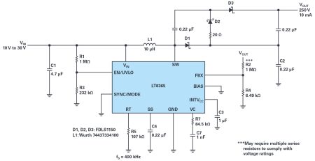
Figure 1. 12V input to 250V output 2-stage boost converter.


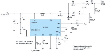
Figure 2. 12V input to –250V output 2-stage inverting converter.

Step-Up Ratios >1:40
One benefit of DCM operation in a boost converter is the ability to achieve a high step-up ratio independent of duty cycle. Additionally, the values and physical sizes of the inductor and output capacitor can be reduced, which leads to a smaller overall footprint solution on the PCB. The circuit in Figure 3 can easily fit in an area less than 1cm2.
There are situations when only a very low input source is available and a high output voltage is needed. The converter shown in Figure 3 could be used to drive a variety of avalanche photo diodes, PIN diodes, and other devices requiring high bias voltages. This boost converter produces 125V from a 3V input source with up to 3mA of load current.

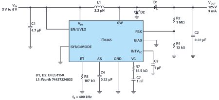
Figure 3. 3V input to 125V output boost converter.

The converter shown in Figure 4 extends the 125V output to 250V from a 3V input source and supports about 1.5mA. There are many devices in the communications field requiring such high bias voltages from low input voltage sources.

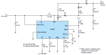
Figure 4. 3V input to 250V output 2-stage boost converter.

How High or Low Can You Go?
For situations where very high voltage is needed, whether positive or negative, a boost converter can use multiplier stages to boost the output 2×, 3×, or more. The converters in Figure 1 and Figure 2 show how to double the switch voltage in both directions, positive and negative. The 3-stage boost converter in Figure 5 delivers 375V at 8mA from a 12V input source.
Note that the available output current must decrease as output voltage increases, since the switch capability does not change. As an example, a single-stage converter designed to deliver 20mA will deliver about 10mA when a second stage is added. As additional stages are added, always ensure the peak switch current stays within the guaranteed switch current limit.

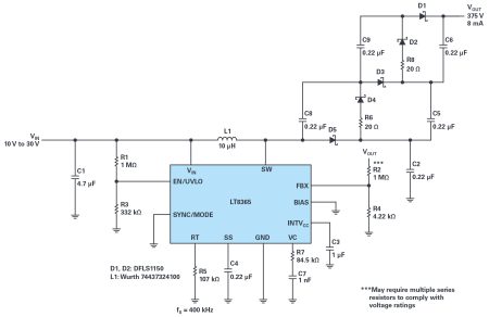
Figure 5. 12V input to 375V output 3-stage boost converter.

Output Voltage Sensing Simplified
The LT8365 offers a single FBX pin to sense the output voltage. A simple resistor divider connected to the FBX pin senses the output voltage, independent of output polarity, as observed on all the schematics presented in this article.
Conclusion
The LT8365 enables applications that require compact, efficient, high output voltage boost conversion from input voltages as low as 2.8V, which is common in the field of communications. It can also be used as an inverting converter and in popular topologies such as CUK and SEPIC converters. The LT8365 is available in a small, thermally enhanced, 16-lead MSOP package.

About the Author
Jesus Rosales is an applications engineer in Analog Devices’ Applications Group in Milpitas, CA. He joined Linear Technology (now a part of ADI) in 1995 as an associate engineer and was promoted to applications engineer in 2001. He has since supported the boost/inverting/SEPIC family of monolithic converters and some offline isolated application controllers. He received an associate degree in electronics from Bay Valley Technical Institute in 1982. He can be reached at jesus.rosales@analog.com.

> Read More

Mouser stocking newest connectivity solutions from Digi International

Mouser stocks more than 600 different products from Digi, in addition to more than 1,000 part numbers available to order. The Digi ConnectCore 93 system-on-module (SoC) provides reliable wireless communication, maximum power efficiency, and enhanced security for embedded devices. Key features include Wi-Fi 6 and Bluetooth® 5.2 connectivity, Arm Cortex-A55 cores, and an AI/ML Arm Ethos U65 neural processing unit.

The new Digi XBee XR 868 RF modules are designed for long-range connectivity applications. The XBee XR 868 radio frequency modules operate in the 863 to 870 MHz frequency range and support point-to-point and mesh networking protocols. Listen Before Talk (LBT) and Adaptive Frequency Agility (AFA) allow the system to assess and adapt to the radio environment, reducing interference.

Mouser also stocks the Digi XBee 3 Global LTE Cat 1 embedded modem, which allows OEMs to incorporate cellular connectivity easily into their device designs. The embedded modem is ideal for a range of IoT applications that require moderate bandwidth and low-cost solutions. The modem is supported by the Digi XBee 3 Global GNSS LTE CAT 1 development kit.

The Digi XBee 3 Global LTE-M/NB-IoT smart modem offers quick time to market, wireless connectivity, and easy-to-add functionality. The XBee 3 Global LTE modules include multiple power-saving features, making them a suitable choice for IoT applications that require low power consumption and long battery life. Digi XCTU software tools simplify setup, configuration, and testing.

https://www.mouser.com/manufacturer/digi-international/

> Read More

PLL/VCO device delivers groundbreaking low phase noise and spur performance

Increasing demands for frequency bandwidth, throughput, and dynamic range in communications systems, together with the need for higher antenna frequencies used in millimetre wave 5G, have all placed further demands on the quality of the local oscillator (LO) or clock used in communications or mixed-signal systems, respectively.

The integrated phase-locked loop (PLL) and voltage controlled oscillator (VCO), the ADF4371, and the similar ADF4372, showcase Analog Devices’ efforts to address the needs of these demanding applications.


Figure 1. ADF4371 block diagram.

Frequency Coverage
To maximise frequency coverage, the ADF4371/ADF4372 VCO covers an octave range from 4GHz to 8GHz, and, by using frequency dividers at the output, dividing by 1/2/4/8/16/32/64 allows full frequency coverage at the main RF8 output of between 62.5MHz to 8000MHz. A second identical output is provided to allow a user to drive a converter clock. The open-loop VCO phase noise is –109dBc/Hz at 100kHz offset for the 8GHz output frequency.
Until recently, generating high frequencies required the use of external frequency multipliers, typically fabricated on GaAs processes, and they often demanded additional filtering, along with amplification, to overcome the effect of the filtering.
To achieve higher frequencies, the ADF4371/ADF4372 contain an integrated frequency doubler, which provides 8GHz to 16GHz output at the differential RF16 pins. The ADF4371 also features a frequency quadrupler that generates from 16GHz to 32GHz at the RF32 differential output. To minimise the generation of unwanted multiplier products, the ADF4371/ADF4372 contain tracking filters that optimise the power level of the desired frequency while suppressing the unwanted multiplier products. On the doubled output, the VCO feedthrough is –45dBc. On the quad output, the suppression is approximately –35dBc.


Figure 2. RMS jitter at 6.144GHz.

Figure 3. RMS jitter at 12.288GHz.

Leading PLL Performance for Converter Clocks
Improvements to the PLL circuitry mean the ADF4371/ADF4372 devices have a PLL figure of merit (FOM) as low as –234dBc/Hz that, when together with a correspondingly low 1/f noise of –127dBc/Hz (normalised to 1GHz output frequency at 10kHz offset), allows users to generate clocks with an rms jitter number as low as 40fs (1kHz to 100MHz integration limit), making them very suitable for use in the most demanding converter clock applications. A simple low-pass filter with small resistors is recommended in order to minimise the resistor noise, which may appear in the loop. A high frequency (250MHz or 125MHz using the reference frequency doubler) ultralow noise reference source is essential for achieving such low noise. The phase frequency detector (PFD) can operate up to a maximum of 250MHz in integer-N applications. The doubled VCO differential output at RF16 can be used to interface directly to some ADI converters without the need for external balun circuitry, which would increase cost and performance. No degradation in performance from 6.144GHz to 12.288GHz is expected.

Communications and Instrumentation LOs
For wireless and instrumentation applications, the ADF4371/ADF4372 contain 39-bit resolution sigma-delta modulators, which enable frequency generation with sub-millihertz resolution with 0Hz error. In this case, the ADF4371 PFD operates up to a maximum of 160MHz PFD frequency. In these applications, the ADF4371/ADF4372 deliver <48fs rms jitter. The ADF4371 also has industry-leading PLL spurious performance, with PFD spurious as low as –100dBc and in-band, unfiltered integer boundary spurious as low as –55dBc. This performance level greatly simplifies frequency planning and reduces time to market. Many fractional-N PLL and VCO devices have unpredictable fractional-N spurious mechanisms, which can lead to additional unplanned characterisation and frequency planning, which add complexity and cost.

Small Size
The ADF4371/ADF4372 PLL/VCO devices are available in 7mm × 7mm, 48-lead land grid array (LGA) packages. Minimal additional decoupling is required, meaning exceptional performance exists in a small footprint solution.
To achieve the best performance, the use of high quality low dropout (LDO) regulators such as the ADM7150 or LT3045 are recommended. The VCO can be supplied with either 3.3V or 5V, and the remaining circuitry is powered from a 3.3V rail. The ADF4371 can be simulated in ADIsimPLL™ to assist the user in designing the appropriate external component circuitry required to implement a full PLL system.

Conclusion
Industry-leading frequency coverage, performance, and small form factor combine on the ADF4371 to address the high demands of new communication and instrumentation systems.

About the Author
Ian Collins graduated from University College Cork with a degree in electrical and electronic engineering, and he has worked in the RF and Microwave Group at Analog Devices since 2000. He is currently an applications manager in the Microwave Frequency Generation Group, which focuses mainly on phase-locked loop (PLL) and voltage controlled oscillator (VCO) products. When not spending time at work or with his young family, Ian enjoys photography and the theatre (both on- and off-stage), reading, and listening to music. He can be reached at ian.collins@analog.com.

> Read More

World’s first resilient SIM, rSIM launches in partnership Deutsche Telekom and Tele2

A new intelligent SIM card that promises to radically improve network connectivity for IoT devices and mobile internet has been launched today in partnership with global operators Deutsche Telekom IoT and Tele2 IoT.

The rSIM (Resilient SIM) uses new patented technology to check its own network connectivity and switch providers automatically when disruptions occur, minimising the chances of the SIM and the device becoming disconnected during outages. With two independent mobile operator profiles stored on the single SIM card, rSIM significantly reduces the risk of outages by switching to a backup mobile operator profile if an outage is detected. The SIM offers two levels of resilience, enabling seamless roaming outside of a device’s home country as well as a proactive solution for uninterrupted internet access. The intelligence is brought to life in a new Connectivity Management Platform, where customers can see real-time connection tests from every SIM no matter which mobile operator profile it is connected to.

Deutsche Telekom IoT and Tele2 IoT will act as rSIM’s first connectivity partners, providing independent operator profiles from within their group to deliver true resilience to a global audience.

rSIM will combine best in-class SIM innovation with patented technology to help mobile operators better serve customers. A global SIM technology provider will lead on the product build and manufacture, as well as providing supporting SIM systems that allow rSIMs to be updated over the air. As part of this they will prioritise GSMA compliance to optimise device and operator compatibility.

The launch of rSIM follows on from a series of notable and high-profile network outages. As Mobile Network Operators (MNOs) invest in upgrading their core networks away from 2G and 3G, to 4G and 5G, periods of unplanned downtime have become more prevalent. A recent outage in Australia left customers disconnected and, in some cases, in life-critical positions. A 12-hour network outage in November 2023 affected over 10 million individuals, resulting in a collapse in the Australian health service and shutting down entire train networks. rSIM provides a real-time solution to mitigate critical connectivity outages and the disruption associated with them.

Richard Cunliffe, Director of Product and Innovation, rSIM, says: “There were around 2 billion cellular IoT connections in 2023, growing to around 7 billion in 2033. As more industries become dependent on IoT, mobile network outages are becoming more commonplace, as more devices connect to them. This increased disruption is affecting all industries, but the biggest impact is seen in critical sectors where lives and infrastructure are at risk, for example in Telecare and Critical National Infrastructure (CNI). Working with our best-in-class global partners on the development, build and rollout of rSIM, our innovative dual SIM, dual core approach will provide a solution which both monitors disruptions and reacts to them at speed.”

rSIM’s innovative approach to standards compliance ensures its adaptability alongside evolving GSMA standards. This will include the development of a version compatible with SGP.32 standards in 2025, which are integral to eSIM remote provisioning for IoT devices, particularly those with network or user interface limitations.

https://www.rsim.com

> Read More

About Smart Cities

This news story is brought to you by smartcitieselectronics.com, the specialist site dedicated to delivering information about what’s new in the Smart City Electronics industry, with daily news updates, new products and industry news. To stay up-to-date, register to receive our weekly newsletters and keep yourself informed on the latest technology news and new products from around the globe. Simply click this link to register here: Smart Cities Registration