Integrated, low power, single-chip LCOS panel fits into AR/XR/MR glasses

The OP03011 liquid crystal on silicon (LCoS) panel integrates the array and frame buffer into an ultra-compact single-chip solution that is lightweight and low-power for smart glasses

The OP03011 is a single chip, 648p LCoS panel for next generation augmented reality (AR), extended reality (XR) and mixed reality (MR) glasses and head-mounted displays. The LCOS panel features 3.8 micron pixels in what is claimed to be one of the world’s smallest 0.14-inch optical formats. The low power, lightweight design is intended for next-generation glasses that can be worn 24/7, said Omnivision.

The growing interest in AR glasses has led OEMs to design more functionality into slim, fashionable designs that consume very little power and are lightweight, allowing them to be worn for long periods. The OP03011 is designed in a compact format for applications requiring a smaller field of view and lower resolution, making it well suited for some of the sleekest, most innovatively designed AR glasses, said Devang Patel, marketing director for the IoT and emerging segment, Omnivision. “The OP03011 supports applications of next-generation smart glasses, like displaying notifications in the user’s field of view and access to GPS for maps and directions directly from the glasses, so the user never needs to pull out their smartphone,” he said.

The OP03011 features 648 x 648 resolution at 120Hz and comes in a small FPCA package. It supports a single-lane MIPI-DSI interface. 

Samples are available now, and the OP03011 will be in mass production in Q4 of 2023.

Omnivision is a fabless semiconductor company that develops advanced digital imaging, analogue and touch and display solutions for multiple applications and industries, including mobile phones, security and surveillance, automotive, computing, medical, and emerging applications. 

http://www.ovt.com

> Read More

Synopsys and Arm push on with next-gen mobile SoC designs

Synopsys combines EDA and IP with Arm’s Total Compute Solutions at Computex Taipei. The AI-enhanced design collaboration tackles mobile chip designs on advanced nodes down to 2nm. At the show, Synopsys announced Synopsys.ai full-stack AI-driven EDA suite, Synopsys Interface and Security IP and Synopsys Silicon Lifecycle Management PVT IP have been optimised for the highest levels of performance and power for Arm’s latest compute platform

These advancements continue the decades of collaboration between the two companies to accelerate customers’ delivery of Arm-based SoCs for smartphones and VR / AR applications.

Shankar Krishnamoorthy, general manager of Synopsys EDA group, commented: “Collaborating with Arm to optimise our EDA and IP solutions enables mutual customers to tackle some of the toughest multi-die system integration challenges from design, IP integration and verification to software development. The addition of the Synopsys.ai EDA suite starts a new phase, where co-operative keystone companies, like Synopsys and Arm, align expertise to help mutual customers turbo-charge the delivery of their Arm-based SoC designs.”

Arm announced its Total Compute Solutions 2023 (TCS23) platform at the show in Taipei. “The new TCS23 platform delivers a suite of segment-specific technology, designed with the system in mind, so that our customers can tap into the compute performance required for the next generation of visual computing experiences,” said Chris Bergey, senior vice president and general manager, client line of business, at Arm.

For TCS23, the Synopsys.ai full-stack AI-driven EDA suite leverages the power of AI from system architecture through manufacturing to optimise power, performance and area (PPA) and enhance time to market, said the company.

The Synopsys Verification family accelerates architecture exploration, software development and verification throughput for Arm SoCs containing Arm Cortex-X4, Cortex-A720 and Cortex-A520 CPUs and Immortalis-G720 and Mali-G720 GPUs. 

Early adopters of TCS23 are using Synopsys virtual prototypes with Arm Fast Models, Synopsys hardware-assisted verification and verification IP for the latest Arm AMBA interconnect to deliver SoCs to market faster.

Synopsys Interface and Security IP for PCI Express 6.0 with Integrity and Data Encryption (IDE), CXL 3.0 with IDE, DDR5 with Inline Memory Encryption (IME) and UCIe, are all optimised for performance with Arm-specific features and for pre-silicon interoperability with Arm cores to minimise risk and to accelerate time to market.

The Synopsys Silicon Lifecycle Management Family PVT monitor IP can be integrated into Arm cores to monitor chip health from development to the field to measure and optimise performance.

Synopsys Fusion QuickStart Implementation Kits (QIKs) are tuned to extract maximum entitlement from the latest five, four and 3nm process technologies. They provide the most efficient path to realising optimally scaled compute architectures for the most demanding end-user applications, said the company.

Synopsys QIKs include implementation scripts and reference guides that enable early adopters of the newest Armv9.2 cores to accelerate time to market and achieve their demanding performance per Watt targets. These QIKs are available today by request through the Arm support hub or from Synopsys SolvNet.

Synopsys also incorporates the latest Arm Fast Models for virtual prototypes and delivers verification IP for the latest Arm AMBA interconnect, emulation and prototyping hardware to accelerate hardware-software bring-up and power and performance validation, resulting in shorter time to market.

Synopsys IP for PCI Express 6.0 with IDE, CXL 3.0 with IDE, DDR5 with IME and UCIe are available now.

http://www.synopsys.com 

> Read More

HD image sensor enables AI face recognition in thin bezel computers

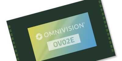
The OV02E 1080p high definition (HD) image sensor has staggered high dynamic range (HDR) and can operate with AI chips to bring always-on ID recognition to notebooks and tablets with thin bezels. The 1/7.3 inch format sensor can be combined with the AI devices to sense human presence in always on, low power mode, to extend the battery life in thse portable devices.

“Our new OV02E is a single-die solution that meets the computing industry’s need for high video quality and low bill of materials (BOM) cost,” said Akeem Chen, product marketing manager, Omnivision. HDR address backlighting issues, for example in video calls where the poor quality backlighting can reduce image quality. “Now, with staggered HDR support, troublesome backlighting during a videoconference call is no longer an issue,” he added.

The sensors new features, such as the low power mode with AI functionality have been added in response to some of the trending features demanded by consumers in 2023 and 2024 laptop models, said Chen.

The OV02E is compact, and suitable for devices with a screen-to-body ratio of less than 3mm Y size, such as tablets and wearable devices. It has a 1.12 micron backside illuminated (BSI) pixel based on Omnivision’s proprietary PureCel Plus architecture for advanced pixel sensitivity and quantum efficiency. The sensor features 2Mpixel, full HD 1080p video at 60 frames per second and supports multiple camera synchronisation for machine vision and IoT applications which require depth detection. The OV02E sensor’s always-on capability has a low power state that works with the mobile industry processor interface (MIPI) and serial peripheral interface (SPI).

Samples of the OV02E are available now, and it will be in mass production in Q4 2023. 

Omnivision is a fabless semiconductor company which develops advanced digital imaging, analogue and touch and display solutions for multiple applications and industries, including mobile phones, security and surveillance, automotive, computing, medical and emerging applications. 

http://www.ovt.com

> Read More

Nanusens shrinks sensor and control circuit for ASICs with embedded sensors

By simultaneously shrinking the sensor and control circuit, Nanusens has created a digital circuit design to measure the capacitance of its nanosensors to create ASICs with integrated sensors. Both the sensor structure and its detection circuitry can be made at the same time within a chip using standard CMOS processes on whatever process node is required, explained the company. As a result, ASICs can now be made with several sensors embedded within them. Integrating sensors as IP blocks offers dramatic reductions in costs and size, claimed Nanusens, as it completely replaces the current solution of discrete sensor packages.

“This is a major milestone for the company,” said Dr. Josep Montanyà, CEO of Nanusens. “The first was successfully making our unique, nanoscale, sensor structures within the CMOS layers. This solves the problem that conventional MEMS have to be made on custom production lines that have limited production capabilities whereas we can make almost unlimited numbers of our sensors in CMOS fabs. These are available in standard packages such as LGA, QFN, WLCSP and others, but, like all other MEMS sensors, they require analogue circuitry to detect tiny capacitance changes coming from nano-displacements of their devices in operation. Our breakthrough is the creation of a fully digital detection circuit as this can be scaled down to the process node being used for the sensor structure and pairs to form a complete sensor and detection solution.

Shrinking the sensor and circuitry simultaneously enables the company to take advantage of smaller CMOS geometries which include reduced costs and reduced power consumption of more than 10 times compared to analogue detection circuits. “This is impossible for other MEMS sensor solutions as their structures cannot be shrunk neither can their analogue circuits as their transistors need a large area to maintain the required low levels of noise,” said Montanyà.

The all-digital detection circuit provides a very fast on / off switching of the circuit of three microseconds compared to 300 microseconds or several milliseconds in conventional analogue transconductance / charge amplifier or similar circuits, said Nanusens. This is advantageous for applications which require a low sampling frequency, such as motion detector applications where the motion detector is typically used to wake up the rest of the device. If the device is in sleep mode most of the time, the battery life is dependent on the current consumption of the motion detector. The fast on / off of the new digital detection circuit results in sub micro A current consumption on the 180nm test chip, which more than doubles the battery life in these applications.

“Instead of being discrete packages on a PCB or a multi-die solution, all the required sensors can be integrated into an ASIC just like another IP block,” said Montanyà. Portable multi-sensor devices, such as smart phones, ear buds and smart watches will benefit from the reduction in BoM, size and power budget and Nanusens confirmed that it is in discussion with companies who want to license this IP.

Founded in 2014, Nanusens is headquartered in Paignton, Devon, England with R & D offices in Barcelona, Spain and Shenzen, China. 

http://www.nanusens.com

> Read More

About Smart Cities

This news story is brought to you by smartcitieselectronics.com, the specialist site dedicated to delivering information about what’s new in the Smart City Electronics industry, with daily news updates, new products and industry news. To stay up-to-date, register to receive our weekly newsletters and keep yourself informed on the latest technology news and new products from around the globe. Simply click this link to register here: Smart Cities Registration